- 您現在的位置:買賣IC網 > PDF目錄371036 > MC74HC259A (Motorola, Inc.) 8-Bit Addressable Latch 1-of-8 Decoder PDF資料下載
參數資料
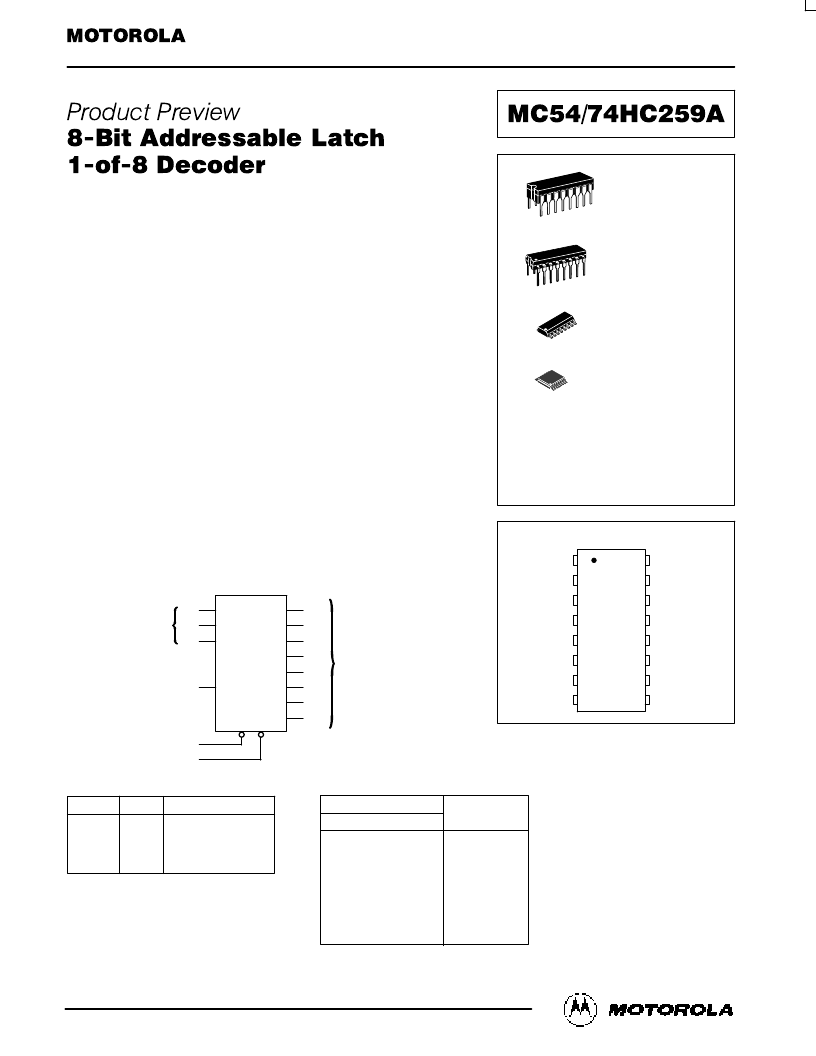
| 型號: | MC74HC259A |
| 廠商: | Motorola, Inc. |
| 英文描述: | 8-Bit Addressable Latch 1-of-8 Decoder |
| 中文描述: | 8位可尋址鎖存1中,8解碼器 |
| 文件頁數: | 1/8頁 |
| 文件大小: | 246K |
| 代理商: | MC74HC259A |
SEMICONDUCTOR TECHNICAL DATA
1
REV 0
Motorola, Inc. 1995
10/95
! !
High–Performance Silicon–Gate CMOS
The MC54/74HC259A is identical in pinout to the LS259. The device
inputs are compatible with standard CMOS outputs; with pullup resistors,
they are compatible with LSTTL outputs.
The HC259A has four modes of operation as shown in the mode selection
table. In the addressable latch mode, the data on Data In is written into the
addressed latch. The addressed latch follows the data input with all
non–addressed latches remaining in their previous states. In the memory
mode, all latches remain in their previous state and are unaffected by the
Data or Address inputs. In the one–of–eight decoding or demultiplexing
mode, the addressed output follows the state of Data In with all other outputs
in the LOW state. In the Reset mode all outputs are LOW and unaffected by
the address and data inputs. When operating the HC259A as an
addressable latch, changing more than one bit of the address could impose
a transient wrong address. Therefore, this should only be done while in the
memory mode.
Output Drive Capability: 10 LSTTL Loads
Outputs Directly Interface to CMOS, NMOS, and TTL
Operating Voltage Range: 2 to 6 V
Low Input Current: 1
μ
A
High Noise Immunity Characteristic of CMOS Devices
In Compliance with the Requirements Defined by JEDEC Standard
No. 7A
Chip Complexity: 202 FETs or 50.5 Equivalent Gates
LOGIC DIAGRAM
ADDRESS
INPUTS
A0
A1
A2
DATA IN
RESET
ENABLE
14
15
13
3
2
1
12
11
10
9
7
6
5
4Q0
Q1
Q2
Q3
Q4
Q5
Q6
Q7
PIN 16 = VCC
PIN 8 = GND
NONINVERTING
OUTPUTS
LATCH SELECTION TABLE
Address Inputs
C
B
Latch
Addressed
A
L
L
L
L
H
H
H
H
L
L
H
H
L
L
H
H
L
H
L
H
L
H
L
H
Q0
Q1
Q2
Q3
Q4
Q5
Q6
Q7
MODE SELECTION TABLE
Enable
Reset
Mode
L
H
L
H
H
H
L
L
Addressable Latch
Memory
8–Line Demultiplexer
Reset
This document contains information on a product under development. Motorola reserves the right to change or discontinue this product without notice.
PIN ASSIGNMENT
13
14
15
16
9
10
11
12
5
4
3
2
1
8
7
6
Q7
DATA IN
ENABLE
RESET
VCC
Q4
Q5
Q6
Q0
A2
A1
A0
GND
Q3
Q2
Q1
D SUFFIX
SOIC PACKAGE
CASE 751B–05
N SUFFIX
PLASTIC PACKAGE
CASE 648–08
ORDERING INFORMATION
MC54HCXXXAJ
MC74HCXXXAN
MC74HCXXXAD
MC74HCXXXADT
Ceramic
Plastic
SOIC
TSSOP
1
16
1
16
J SUFFIX
CERAMIC PACKAGE
CASE 620–10
1
16
1
16
DT SUFFIX
TSSOP PACKAGE
CASE 948F–01
相關PDF資料 |
PDF描述 |
|---|---|
| MC74HC259AD | 8-Bit Addressable Latch 1-of-8 Decoder |
| MC74HC259ADT | 8-Bit Addressable Latch 1-of-8 Decoder |
| MC74HC259AN | 8-Bit Addressable Latch 1-of-8 Decoder |
| MC54-74HC273A | Octal D Flip-Flop with Common Clock and Reset |
| MC7HC273A | Octal D Flip-Flop with Common Clock and Reset |
相關代理商/技術參數 |
參數描述 |
|---|---|
| MC74HC259ADG | 功能描述:編碼器、解碼器、復用器和解復用器 IC MULTIPLEXER 3ST 8INPUT RoHS:否 制造商:Micrel 產品:Multiplexers 邏輯系列:CMOS 位數: 線路數量(輸入/輸出):2 / 12 傳播延遲時間:350 ps, 400 ps 電源電壓-最大:2.625 V, 3.6 V 電源電壓-最小:2.375 V, 3 V 最大工作溫度:+ 85 C 安裝風格:SMD/SMT 封裝 / 箱體:QFN-44 封裝:Tray |
| MC74HC259ADR2G | 功能描述:編碼器、解碼器、復用器和解復用器 IC MULTIPLEXER RoHS:否 制造商:Micrel 產品:Multiplexers 邏輯系列:CMOS 位數: 線路數量(輸入/輸出):2 / 12 傳播延遲時間:350 ps, 400 ps 電源電壓-最大:2.625 V, 3.6 V 電源電壓-最小:2.375 V, 3 V 最大工作溫度:+ 85 C 安裝風格:SMD/SMT 封裝 / 箱體:QFN-44 封裝:Tray |
| MC74HC259ADTG | 功能描述:編碼器、解碼器、復用器和解復用器 IC MULTIPLEXER 3ST 8INPUT RoHS:否 制造商:Micrel 產品:Multiplexers 邏輯系列:CMOS 位數: 線路數量(輸入/輸出):2 / 12 傳播延遲時間:350 ps, 400 ps 電源電壓-最大:2.625 V, 3.6 V 電源電壓-最小:2.375 V, 3 V 最大工作溫度:+ 85 C 安裝風格:SMD/SMT 封裝 / 箱體:QFN-44 封裝:Tray |
| MC74HC259ADTR2 | 制造商:Rochester Electronics LLC 功能描述:- Bulk 制造商:ON Semiconductor 功能描述: |
| MC74HC259ADTR2G | 功能描述:編碼器、解碼器、復用器和解復用器 IC MULTIPLEXER 3ST 8INPUT RoHS:否 制造商:Micrel 產品:Multiplexers 邏輯系列:CMOS 位數: 線路數量(輸入/輸出):2 / 12 傳播延遲時間:350 ps, 400 ps 電源電壓-最大:2.625 V, 3.6 V 電源電壓-最小:2.375 V, 3 V 最大工作溫度:+ 85 C 安裝風格:SMD/SMT 封裝 / 箱體:QFN-44 封裝:Tray |
發布緊急采購,3分鐘左右您將得到回復。