- 您現(xiàn)在的位置:買賣IC網(wǎng) > PDF目錄371065 > MC74HC4052A (Motorola, Inc.) ANALOG MULTIPLEXERS/ DEMULTIPLEXERS PDF資料下載
參數(shù)資料
| 型號: | MC74HC4052A |
| 廠商: | Motorola, Inc. |
| 英文描述: | ANALOG MULTIPLEXERS/ DEMULTIPLEXERS |
| 中文描述: | 模擬多路復(fù)用器/解復(fù)用器 |
| 文件頁數(shù): | 10/15頁 |
| 文件大小: | 199K |
| 代理商: | MC74HC4052A |
MC54/74HC4051A MC74HC4052A MC54/74HC4053A
MOTOROLA
High–Speed CMOS Logic Data
DL129 — Rev 6
10
RL
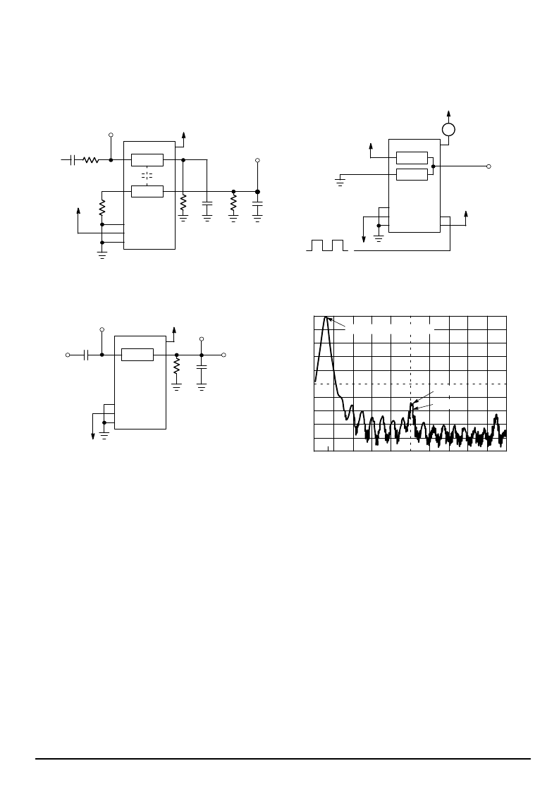
Figure 12. Crosstalk Between Any Two
Switches, Test Set–Up
Figure 13. Power Dissipation Capacitance,
Test Set–Up
Figure 14a. Total Harmonic Distortion, Test Set–Up
Figure 14b. Plot, Harmonic Distortion
0
–10
–20
–30
–40
–50
–100
1.0
2.0
3.125
FREQUENCY (kHz)
d
–60
–70
–80
–90
FUNDAMENTAL FREQUENCY
DEVICE
SOURCE
ON
6
7
8
16
VEE
CL*
*Includes all probe and jig capacitance
OFF
RL
RL
VIS
RL
CL*
VOS
fin
0.1
μ
F
ON/OFF
6
7
8
16
VCC
CHANNEL SELECT
NC
COMMON O/I
OFF/ON
ANALOG I/O
VCC
A
11
VCC
VEE
ON
6
7
8
16
VCC
VEE
0.1
μ
F
CL*
fin
RL
TO
DISTORTION
METER
*Includes all probe and jig capacitance
VOS
VIS
APPLICATIONS INFORMATION
The Channel Select and Enable control pins should be at
VCC or GND logic levels. VCC being recognized as a logic
high and GND being recognized as a logic low. In this exam-
ple:
VCC = +5V = logic high
GND = 0V = logic low
The maximum analog voltage swings are determined by
the supply voltages VCC and VEE. The positive peak analog
voltage should not exceed VCC. Similarly, the negative peak
analog voltage should not go below VEE. In this example, the
difference between VCC and VEE is ten volts. Therefore,
using the configuration of Figure 15, a maximum analog sig-
nal of ten volts peak–to–peak can be controlled. Unused
analog inputs/outputs may be left floating (i.e., not con-
nected). However, tying unused analog inputs and outputs to
VCC or GND through a low value resistor helps minimize
crosstalk and feedthrough noise that may be picked up by an
unused switch.
Although used here, balanced supplies are not a require-
ment. The only constraints on the power supplies are that:
VCC – GND = 2 to 6 volts
VEE – GND = 0 to –6 volts
VCC – VEE = 2 to 12 volts
and VEE
≤
GND
When voltage transients above VCC and/or below VEE are
anticipated on the analog channels, external Germanium or
Schottky diodes (Dx) are recommended as shown in Figure
16. These diodes should be able to absorb the maximum
anticipated current surges during clipping.
相關(guān)PDF資料 |
PDF描述 |
|---|---|
| MC74HC4066D | Adjustable/2.5V, 0.5% Tolerance Shunt Regulator; Package: SOIC; No of Pins: 8; Container: Tape & Reel |
| MC74HC4066N | Quad Analog Switch/Multiplexer/Demultiplexer |
| MC74HC4075D | Triple 3-Input OR Gate |
| MC74HC4075N | Triple 3-Input OR Gate |
| MC74HC4075 | TRIPLE 3- INPUT OR GATE HIGH-PERFORMANCE SILICON-GATE CMOS |
相關(guān)代理商/技術(shù)參數(shù) |
參數(shù)描述 |
|---|---|
| MC74HC4052AD | 功能描述:多路器開關(guān) IC 2-6V ANLG Mux/Demux RoHS:否 制造商:Texas Instruments 通道數(shù)量:1 開關(guān)數(shù)量:4 開啟電阻(最大值):7 Ohms 開啟時間(最大值): 關(guān)閉時間(最大值): 傳播延遲時間:0.25 ns 工作電源電壓:2.3 V to 3.6 V 工作電源電流: 最大工作溫度:+ 85 C 安裝風格:SMD/SMT 封裝 / 箱體:UQFN-16 |
| MC74HC4052ADG | 功能描述:多路器開關(guān) IC 2-6V ANLG Mux/Demux -55 to 125deg C RoHS:否 制造商:Texas Instruments 通道數(shù)量:1 開關(guān)數(shù)量:4 開啟電阻(最大值):7 Ohms 開啟時間(最大值): 關(guān)閉時間(最大值): 傳播延遲時間:0.25 ns 工作電源電壓:2.3 V to 3.6 V 工作電源電流: 最大工作溫度:+ 85 C 安裝風格:SMD/SMT 封裝 / 箱體:UQFN-16 |
| MC74HC4052ADR2 | 功能描述:多路器開關(guān) IC 2-6V ANLG Mux/Demux RoHS:否 制造商:Texas Instruments 通道數(shù)量:1 開關(guān)數(shù)量:4 開啟電阻(最大值):7 Ohms 開啟時間(最大值): 關(guān)閉時間(最大值): 傳播延遲時間:0.25 ns 工作電源電壓:2.3 V to 3.6 V 工作電源電流: 最大工作溫度:+ 85 C 安裝風格:SMD/SMT 封裝 / 箱體:UQFN-16 |
| MC74HC4052ADR2G | 功能描述:多路器開關(guān) IC 2-6V ANLG Mux/Demux -55 to 125deg C RoHS:否 制造商:Texas Instruments 通道數(shù)量:1 開關(guān)數(shù)量:4 開啟電阻(最大值):7 Ohms 開啟時間(最大值): 關(guān)閉時間(最大值): 傳播延遲時間:0.25 ns 工作電源電壓:2.3 V to 3.6 V 工作電源電流: 最大工作溫度:+ 85 C 安裝風格:SMD/SMT 封裝 / 箱體:UQFN-16 |
| MC74HC4052ADR2G-CUT TAPE | 制造商:ON 功能描述:MC74HC4052A Series 2 to 6 V Analog Multiplexers / Demultiplexers - SOIC-16 |
發(fā)布緊急采購,3分鐘左右您將得到回復(fù)。