- 您現在的位置:買賣IC網 > PDF目錄382311 > MC74LVX4053DTR2 (ON SEMICONDUCTOR) Analog Multiplexer/ Demultiplexer High?Performance Silicon?Gate CMOS PDF資料下載
參數資料
| 型號: | MC74LVX4053DTR2 |
| 廠商: | ON SEMICONDUCTOR |
| 元件分類: | 運動控制電子 |
| 英文描述: | Analog Multiplexer/ Demultiplexer High?Performance Silicon?Gate CMOS |
| 中文描述: | TRIPLE 2-CHANNEL, SGL ENDED MULTIPLEXER, PDSO16 |
| 封裝: | TSSOP-16 |
| 文件頁數: | 11/16頁 |
| 文件大小: | 141K |
| 代理商: | MC74LVX4053DTR2 |
MC74LVX4053
http://onsemi.com
11
APPLICATIONS INFORMATION
The Channel Select and Enable control pins should be at
V
CC
or GND logic levels. V
CC
being recognized as a logic
high and GND being recognized as a logic low. In this
example:
V
CC
=
5 V = logic high
GND = 0 V = logic low
The maximum analog voltage swing is determined by the
supply voltages V
CC
and V
EE
. The positive peak analog
voltage should not exceed V
CC
. Similarly, the negative peak
analog voltage should not go below V
EE
. In this example,
the difference between V
CC
and V
EE
is five volts. Therefore,
using the configuration of Figure 21, a maximum analog
signal of five volts peak–to–peak can be controlled. Unused
analog inputs/outputs may be left floating (i.e., not
connected). However, tying unused analog inputs and
outputs to V
CC
or GND through a low value resistor helps
minimize crosstalk and feedthrough noise that may be
picked up by an unused switch.
Although used here, balanced supplies are not a
requirement. The only constraints on the power supplies are
that:
V
EE
– GND = 0 to
V
CC
– GND = 2.5 to 6 volts
V
CC
– V
EE
= 2.5 to 6 volts
and V
EE
When voltage transients above V
CC
and/or below V
EE
are
anticipated on the analog channels, external Germanium or
Schottky diodes (D
x
) are recommended as shown in
Figure 22. These diodes should be able to absorb the
maximum anticipated current surges during clipping.
6 volts
GND
ANALOG
SIGNAL
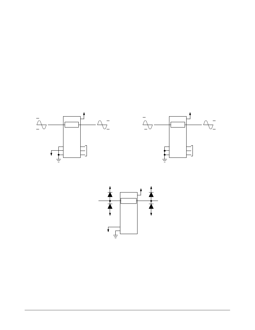
Figure 20. Application Example
ON
6
7
8
16
+3.0 V
ANALOG
SIGNAL
+3.0 V
–3.0 V
+3.0 V
–3.0 V
11
10
9
TO EXTERNAL CMOS
CIRCUITRY 0 to 3.0 V
DIGITAL SIGNALS
–3.0 V
Figure 21. Application Example
ANALOG
SIGNAL
ON
6
7
8
16
+5 V
ANALOG
SIGNAL
+5 V
GND
+5 V
GND
11
10
9
TO EXTERNAL CMOS
CIRCUITRY 0 to 5 V
DIGITAL SIGNALS
ON/OFF
7
8
16
V
CC
V
EE
D
x
V
CC
D
x
V
EE
D
x
V
CC
D
x
V
EE
Figure 22. External Germanium or Schottky Clipping Diodes
相關PDF資料 |
PDF描述 |
|---|---|
| MC74LVX4066 | Quad Analog Switch/Multiplexer/Demultiplexer |
| MC74LVX4066D | Quad Analog Switch/Multiplexer/Demultiplexer |
| MC74LVX4066DR2 | Quad Analog Switch/Multiplexer/Demultiplexer |
| MC74LVX4066DT | Quad Analog Switch/Multiplexer/Demultiplexer |
| MC74LVX4066DTR2 | Quad Analog Switch/Multiplexer/Demultiplexer |
相關代理商/技術參數 |
參數描述 |
|---|---|
| MC74LVX4053DTR2G | 功能描述:多路器開關 IC 2.5-6V Analog Mux/DeMux RoHS:否 制造商:Texas Instruments 通道數量:1 開關數量:4 開啟電阻(最大值):7 Ohms 開啟時間(最大值): 關閉時間(最大值): 傳播延遲時間:0.25 ns 工作電源電壓:2.3 V to 3.6 V 工作電源電流: 最大工作溫度:+ 85 C 安裝風格:SMD/SMT 封裝 / 箱體:UQFN-16 |
| MC74LVX4053M | 功能描述:多路器開關 IC 2.5-6V Analog RoHS:否 制造商:Texas Instruments 通道數量:1 開關數量:4 開啟電阻(最大值):7 Ohms 開啟時間(最大值): 關閉時間(最大值): 傳播延遲時間:0.25 ns 工作電源電壓:2.3 V to 3.6 V 工作電源電流: 最大工作溫度:+ 85 C 安裝風格:SMD/SMT 封裝 / 箱體:UQFN-16 |
| MC74LVX4053MEL | 功能描述:多路器開關 IC 2.5-6V Analog RoHS:否 制造商:Texas Instruments 通道數量:1 開關數量:4 開啟電阻(最大值):7 Ohms 開啟時間(最大值): 關閉時間(最大值): 傳播延遲時間:0.25 ns 工作電源電壓:2.3 V to 3.6 V 工作電源電流: 最大工作溫度:+ 85 C 安裝風格:SMD/SMT 封裝 / 箱體:UQFN-16 |
| MC74LVX4053MELG | 功能描述:多路器開關 IC 2.5-6V Analog Mux/DeMux RoHS:否 制造商:Texas Instruments 通道數量:1 開關數量:4 開啟電阻(最大值):7 Ohms 開啟時間(最大值): 關閉時間(最大值): 傳播延遲時間:0.25 ns 工作電源電壓:2.3 V to 3.6 V 工作電源電流: 最大工作溫度:+ 85 C 安裝風格:SMD/SMT 封裝 / 箱體:UQFN-16 |
| MC74LVX4053MG | 功能描述:多路器開關 IC 2.5-6V Analog Mux/DeMux RoHS:否 制造商:Texas Instruments 通道數量:1 開關數量:4 開啟電阻(最大值):7 Ohms 開啟時間(最大值): 關閉時間(最大值): 傳播延遲時間:0.25 ns 工作電源電壓:2.3 V to 3.6 V 工作電源電流: 最大工作溫度:+ 85 C 安裝風格:SMD/SMT 封裝 / 箱體:UQFN-16 |
發布緊急采購,3分鐘左右您將得到回復。