- 您現在的位置:買賣IC網 > PDF目錄385571 > MC74VHC1GT126 (ON SEMICONDUCTOR) Noninverting Buffer / CMOS Logic Level Shifter(非反相緩沖器) PDF資料下載
參數資料
| 型號: | MC74VHC1GT126 |
| 廠商: | ON SEMICONDUCTOR |
| 英文描述: | Noninverting Buffer / CMOS Logic Level Shifter(非反相緩沖器) |
| 中文描述: | 同相緩沖/ CMOS邏輯電平轉換器(非反相緩沖器) |
| 文件頁數: | 1/8頁 |
| 文件大小: | 104K |
| 代理商: | MC74VHC1GT126 |
Semiconductor Components Industries, LLC, 2002
March, 2002 – Rev. 8
1
Publication Order Number:
MC74VHC1GT126/D
MC74VHC1GT126
Noninverting Buffer /
CMOS Logic Level Shifter
with LSTTL–Compatible Inputs
The MC74VHC1GT126 is a single gate noninverting 3–state buffer
fabricated with silicon gate CMOS technology. It achieves high speed
operation similar to equivalent Bipolar Schottky TTL while maintaining
CMOS low power dissipation.
The MC74VHC1GT126 requires the 3–state control input (OE) to be
set Low to place the output into the high impedance state.
The device input is compatible with TTL–type input thresholds and the
output has a full 5 V CMOS level output swing. The input protection
circuitry on this device allows overvoltage tolerance on the input,
allowing the device to be used as a logic–level translator from 3.0 V
CMOS logic to 5.0 V CMOS Logic or from 1.8 V CMOS logic to 3.0 V
CMOS Logic while operating at the high–voltage power supply.
The MC74VHC1GT126 input structure provides protection when
voltages up to 7V are applied, regardless of the supply voltage. This
allows the MC74VHC1GT126 to be used to interface 5 V circuits to 3 V
circuits. The output structures also provide protection when VCC = 0 V.
These input and output structures help prevent device destruction caused
by supply voltage – input/output voltage mismatch, battery backup, hot
insertion, etc.
High Speed: tPD = 3.5 ns (Typ) at VCC = 5 V
Low Power Dissipation: ICC = 1
μ
A (Max) at TA = 25
°
C
TTL–Compatible Inputs: VIL = 0.8 V; VIH = 2.0 V
CMOS–Compatible Outputs: VOH > 0.8 VCC; VOL < 0.1 VCC @Load
Power Down Protection Provided on Inputs and Outputs
Balanced Propagation Delays
Pin and Function Compatible with Other Standard Logic Families
Chip Complexity: FETs = 62; Equivalent
Gates = 16
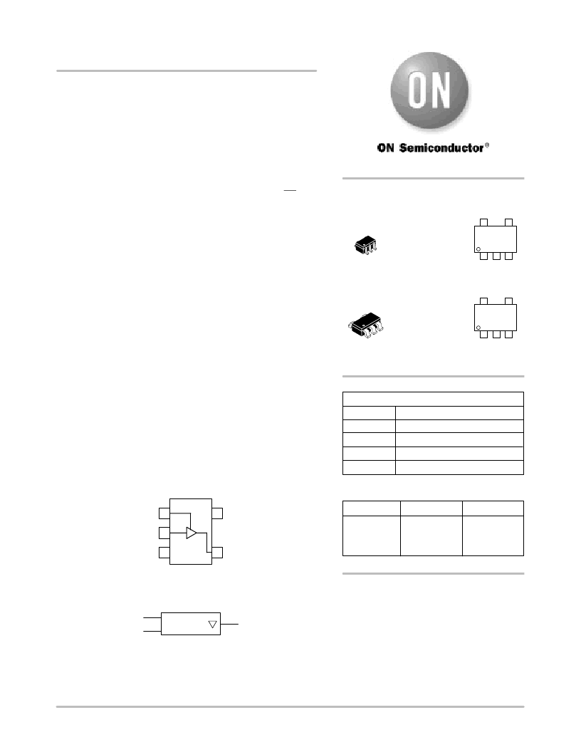
Figure 1. Pinout
(Top View)
IN A
OUT Y
VCC
OE
IN A
OUT Y
GND
OE
Figure 2. Logic Symbol
1
2
3
4
5
PIN ASSIGNMENT
1
2
3
GND
OE
IN A
4
5
VCC
OUT Y
See detailed ordering and shipping information in the package
dimensions section on page 4 of this data sheet.
ORDERING INFORMATION
FUNCTION TABLE
L
H
X
A Input
Y Output
L
H
Z
OE Input
H
H
L
SC–88A / SOT–353/SC–70
DF SUFFIX
CASE 419A
Pin 1
d = Date Code
W3d
TSOP–5/SOT–23/SC–59
DT SUFFIX
CASE 483
Pin 1
d = Date Code
W3d
MARKING
DIAGRAMS
http://onsemi.com
相關PDF資料 |
PDF描述 |
|---|---|
| MC74VHC1GT14DFT1 | Schmitt-Trigger Inverter/CMOS Logic Level Shifter |
| MC74VHC1GT14DFT2 | Schmitt-Trigger Inverter/CMOS Logic Level Shifter |
| MC74VHC1GT14DTT1 | Schmitt-Trigger Inverter/CMOS Logic Level Shifter |
| MC74VHC1GT14 | Schmitt-Trigger Inverter / CMOS Logic Level Shifter(施密特觸發反相器) |
| MC74VHC1GT32 | 2-Input OR Gate/CMOS Logic Level Shifter(雙輸入或門) |
相關代理商/技術參數 |
參數描述 |
|---|---|
| MC74VHC1GT126D1G | 功能描述:緩沖器和線路驅動器 3-5.5V Single Non-Inverting TTL RoHS:否 制造商:Micrel 輸入線路數量:1 輸出線路數量:2 極性:Non-Inverting 電源電壓-最大:+/- 5.5 V 電源電壓-最小:+/- 2.37 V 最大工作溫度:+ 85 C 安裝風格:SMD/SMT 封裝 / 箱體:MSOP-8 封裝:Reel |
| MC74VHC1GT126D1G-CUT TAPE | 制造商:ON 功能描述:MC74VHC1GT126 Series 3 to 5.5 V Noninverting Buffer - Level Shifter - SOT-23-5 |
| MC74VHC1GT126DF1 | 功能描述:緩沖器和線路驅動器 3-5.5V Single RoHS:否 制造商:Micrel 輸入線路數量:1 輸出線路數量:2 極性:Non-Inverting 電源電壓-最大:+/- 5.5 V 電源電壓-最小:+/- 2.37 V 最大工作溫度:+ 85 C 安裝風格:SMD/SMT 封裝 / 箱體:MSOP-8 封裝:Reel |
| MC74VHC1GT126DF1G | 制造商:ON Semiconductor 功能描述:IC LOGIC 74VHC1G BUFFER SC705 制造商:ON Semiconductor 功能描述:IC, LOGIC, 74VHC1G, BUFFER, SC705 |
| MC74VHC1GT126DF2 | 功能描述:緩沖器和線路驅動器 LOG CMOS BUFR NINVERT RoHS:否 制造商:Micrel 輸入線路數量:1 輸出線路數量:2 極性:Non-Inverting 電源電壓-最大:+/- 5.5 V 電源電壓-最小:+/- 2.37 V 最大工作溫度:+ 85 C 安裝風格:SMD/SMT 封裝 / 箱體:MSOP-8 封裝:Reel |
發布緊急采購,3分鐘左右您將得到回復。