- 您現在的位置:買賣IC網 > PDF目錄383570 > MC74VHC1GT86DFT1 (樂山無線電股份有限公司) 2-Input Exclusive OR Gate/CMOS Logic Level Shifter PDF資料下載
參數資料
| 型號: | MC74VHC1GT86DFT1 |
| 廠商: | 樂山無線電股份有限公司 |
| 英文描述: | 2-Input Exclusive OR Gate/CMOS Logic Level Shifter |
| 中文描述: | 2輸入異或門/ CMOS邏輯電平轉換器 |
| 文件頁數: | 1/4頁 |
| 文件大小: | 204K |
| 代理商: | MC74VHC1GT86DFT1 |
LESHAN RADIO COMPANY, LTD.
VHT86–1/4
VM
d
VM
d
1
3
2
4
5
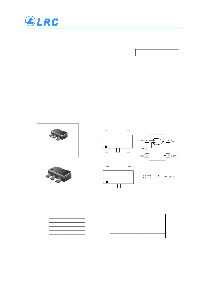
SOT–23/TSOP–5/SC–59
DT SUFFIX
CASE 483
SC–70/SC–88A/SOT–353
DF SUFFIX
CASE 419A
1
3
2
4
5
MARKING DIAGRAMS
Pin 1
d = Date Code
Pin 1
d = Date Code
Figure 1. Pinout
(Top View)
Figure 2. Logic Symbol
PIN ASSIGNMENT
1
2
3
4
5
IN B
IN A
GND
OUT Y
V
CC
FUNCTION TABLE
Inputs
Output
Y
L
H
H
L
A
L
L
H
H
B
L
H
L
H
ORDERING INFORMATION
See detailed ordering and shipping information in the
package dimensions section on page 4 of this data sheet.
2-Input Exclusive OR Gate / CMOS Logic Level Shifter
with LSTTL–Compatible Inputs
The MC74VHC1GT86 is an advanced high speed CMOS 2–input Exclusive OR gate fabricated with silicon gate CMOS technology.
It achieves high speed operation similar to equivalent Bipolar Schottky TTL while maintaining CMOS low power dissipation.
The internal circuit is composed of three stages, including a buffer output which provides high noise immunity and stable output.
The device input is compatible with TTL–type input thresholds and the output has a full 5 V CMOS level output swing. The input
protection circuitry on this device allows overvoltage tolerance on the input, allowing the device to be used as a logic–level translator from
3.0 V CMOS logic to 5.0V CMOS Logic or from 1.8 V CMOS logic to 3.0 V CMOS Logic while operating at the high–voltage power supply.
The MC74VHC1GT86 input structure provides protection when voltages up to 7 V are applied, regardless of the supply voltage. This
allows the MC74VHC1GT86 to be used to interface 5 V circuits to 3 V circuits. The output structures also provide protection when
V
CC
= 0 V. These input and output structures help prevent device destruction caused by supply voltage – input/output voltage mismatch,
battery backup, hot insertion, etc.
High Speed: t
PD
= 4.8 ns (Typ) at V
CC
= 5 V
Low Power Dissipation: I
CC
= 2 mA (Max) at T
A
= 25°C
TTL–Compatible Inputs: V
IL
= 0.8 V; V
IH
= 2.0 V
CMOS–Compatible Outputs: V
OH
> 0.8 V
CC
;
V
OL
< 0.1 V
CC
@Load
MC74VHC1GT86
Power Down Protection Provided on Inputs and Outputs
Balanced Propagation Delays
Pin and Function Compatible with Other Standard Logic Families
Chip Complexity: FETs = 83; Equivalent Gates = 16
相關PDF資料 |
PDF描述 |
|---|---|
| MC74VHC1GT86DFT2 | 2-Input Exclusive OR Gate/CMOS Logic Level Shifter |
| MC74VHC1GT86DFT4 | 2-Input Exclusive OR Gate/CMOS Logic Level Shifter |
| MC74VHC1GT86DTT1 | 2-Input Exclusive OR Gate/CMOS Logic Level Shifter |
| MC74VHC1GT86DTT3 | 2-Input Exclusive OR Gate/CMOS Logic Level Shifter |
| MC74VHC1GU04DFT1 | Unbuffered Inverter |
相關代理商/技術參數 |
參數描述 |
|---|---|
| MC74VHC1GT86DFT2 | 功能描述:邏輯門 3-5.5V Single XOR RoHS:否 制造商:Texas Instruments 產品:OR 邏輯系列:LVC 柵極數量:2 線路數量(輸入/輸出):2 / 1 高電平輸出電流:- 16 mA 低電平輸出電流:16 mA 傳播延遲時間:3.8 ns 電源電壓-最大:5.5 V 電源電壓-最小:1.65 V 最大工作溫度:+ 125 C 安裝風格:SMD/SMT 封裝 / 箱體:DCU-8 封裝:Reel |
| MC74VHC1GT86DT1G | 功能描述:邏輯門 3-5.5V Single XOR 2-Input TTL RoHS:否 制造商:Texas Instruments 產品:OR 邏輯系列:LVC 柵極數量:2 線路數量(輸入/輸出):2 / 1 高電平輸出電流:- 16 mA 低電平輸出電流:16 mA 傳播延遲時間:3.8 ns 電源電壓-最大:5.5 V 電源電壓-最小:1.65 V 最大工作溫度:+ 125 C 安裝風格:SMD/SMT 封裝 / 箱體:DCU-8 封裝:Reel |
| MC74VHC1GT86DTT1 | 功能描述:邏輯門 3-5.5V Single XOR RoHS:否 制造商:Texas Instruments 產品:OR 邏輯系列:LVC 柵極數量:2 線路數量(輸入/輸出):2 / 1 高電平輸出電流:- 16 mA 低電平輸出電流:16 mA 傳播延遲時間:3.8 ns 電源電壓-最大:5.5 V 電源電壓-最小:1.65 V 最大工作溫度:+ 125 C 安裝風格:SMD/SMT 封裝 / 箱體:DCU-8 封裝:Reel |
| MC74VHC1GU04DF1G | 功能描述:變換器 LOG CMOS INVERTER GATE RoHS:否 制造商:NXP Semiconductors 電路數量:6 邏輯系列:74ABT 邏輯類型:BiCMOS 高電平輸出電流:- 15 mA 低電平輸出電流:20 mA 傳播延遲時間:2.2 ns 電源電壓-最大:5.5 V 電源電壓-最小:4.5 V 最大工作溫度:+ 85 C 最小工作溫度:- 40 C 工作溫度范圍: 封裝 / 箱體:DIP-14 封裝:Tube |
| MC74VHC1GU04DF2G | 制造商:Rochester Electronics LLC 功能描述:- Bulk |
發布緊急采購,3分鐘左右您將得到回復。