- 您現在的位置:買賣IC網 > PDF目錄371084 > MCM6227BJ17R2 (MOTOROLA INC) 1M x 1 Bit Static Random Access Memory PDF資料下載
參數資料
| 型號: | MCM6227BJ17R2 |
| 廠商: | MOTOROLA INC |
| 元件分類: | DRAM |
| 英文描述: | 1M x 1 Bit Static Random Access Memory |
| 中文描述: | 1M X 1 STANDARD SRAM, 17 ns, PDSO28 |
| 封裝: | 0.300 INCH, SOJ-28 |
| 文件頁數: | 3/8頁 |
| 文件大小: | 147K |
| 代理商: | MCM6227BJ17R2 |
MCM6227B
3
MOTOROLA FAST SRAM
CAPACITANCE
(f = 1.0 MHz, dV = 3.0 V, TA = 25
°
C, Periodically Sampled Rather Than 100% Tested)
Characteristic
Symbol
Typ
Max
Unit
Input Capacitance
All Inputs Except Clocks and D, Q
E and W
Cin
4
5
6
8
pF
Input and Output Capacitance
D, Q
Cin, Cout
5
8
pF
AC OPERATING CONDITIONS AND CHARACTERISTICS
(VCC = 5.0 V
±
10%, TA = 0 to + 70
°
C, Unless Otherwise Noted)
0 to 3.0 V
. . . . . . . . . . . . . . . . . . . . . . . . . . . . . . . . .
Input Rise/Fall Time
. . . . . . . . . . . . . . . . . . . . . . . . . . . . . . . . . . . .
Input Timing Measurement Reference Level
. . . . . . . . . . . . . . .
Input Pulse Levels
2 ns
1.5 V
Output Timing Measurement Reference Level
Output Load
. . . . . . . . . . . . . . . . . . . . . . . . . . . . . . . . . .
1.5 V
. . . . . . . . . . . . .
See Figure 1a
READ CYCLE TIMING
(See Notes 1 and 2)
6227B–15
6227B–17
6227B–20
6227B–25
6227B–35
Parameter
Symbol
Min
Max
Min
Max
Min
Max
Min
Max
Min
Max
Unit
Notes
Read Cycle Time
tAVAV
tAVQV
tELQV
tAXQX
15
—
17
—
20
—
25
—
35
—
ns
2, 3
Address Access Time
—
15
—
17
—
20
—
25
—
35
ns
Enable Access Time
—
15
—
17
—
20
—
25
—
35
ns
4
Output Hold from
Address Change
5
—
5
—
5
—
5
—
5
—
ns
Enable Low to Output
Active
tELQX
5
—
5
—
5
—
5
—
5
—
ns
5, 6, 7
Enable High to Output
High–Z
tEHQZ
—
6
—
7
—
7
—
8
—
8
ns
5, 6, 7
NOTES:
1. W is high for read cycle.
2. Product sensitivities to noise require proper grounding and decoupling of power supplies as well as minimization or elimination of bus con-
tention conditions during read and write cycles.
3. All timings are referenced from the last valid address to the first transitioning address.
4. Addresses valid prior to or coincident with E going low.
5. At any given voltage and temperature, tEHQZ max is less than tELQX min, both for a given device and from device to device.
6. Transition is measured
±
500 mV from steady–state voltage with load of Figure 1b.
7. This parameter is sampled and not 100% tested.
8. Device is continuously selected (E
≤
VIL).
(a)
(b)
The table of timing values shows either a
minimum or a maximum limit for each param-
eter. Input requirements are specified from
the external system point of view. Thus, ad-
dress setup time is shown as a minimum
since the system must supply at least that
much time. On the other hand, responses
from the memory are specified from the de-
vice point of view. Thus, the access time is
shown as a maximum since the device never
provides data later than that time.
TIMING LIMITS
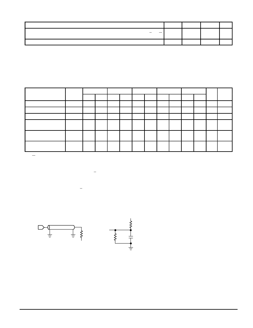
OUTPUT
Z0 = 50
RL = 50
VL = 1.5 V
5 pF
+ 5 V
OUTPUT
255
480
Figure 1. AC Test Loads
相關PDF資料 |
PDF描述 |
|---|---|
| MCM6227BJ20 | 1M x 1 Bit Static Random Access Memory |
| MCM6227BJ20R2 | 1M x 1 Bit Static Random Access Memory |
| MCM6227BJ25 | 1M x 1 Bit Static Random Access Memory |
| MCM6227BJ25R2 | 1M x 1 Bit Static Random Access Memory |
| MCM6227BJ35 | 1M x 1 Bit Static Random Access Memory |
相關代理商/技術參數 |
參數描述 |
|---|---|
| MCM6227BJ20 | 制造商:MOTOROLA 制造商全稱:Motorola, Inc 功能描述:1M x 1 Bit Static Random Access Memory |
| MCM6227BJ20R2 | 制造商:MOTOROLA 制造商全稱:Motorola, Inc 功能描述:1M x 1 Bit Static Random Access Memory |
| MCM6227BJ25 | 制造商:MOTOROLA 制造商全稱:Motorola, Inc 功能描述:1M x 1 Bit Static Random Access Memory |
| MCM6227BJ25R2 | 制造商:MOTOROLA 制造商全稱:Motorola, Inc 功能描述:1M x 1 Bit Static Random Access Memory |
| MCM6227BJ35 | 制造商:MOTOROLA 制造商全稱:Motorola, Inc 功能描述:1M x 1 Bit Static Random Access Memory |
發布緊急采購,3分鐘左右您將得到回復。