- 您現在的位置:買賣IC網 > PDF目錄371087 > MCM63P631ATQ66R (MOTOROLA INC) 64K x 32 Bit Pipelined BurstRAM Synchronous Fast Static RAM PDF資料下載
參數資料
| 型號: | MCM63P631ATQ66R |
| 廠商: | MOTOROLA INC |
| 元件分類: | SRAM |
| 英文描述: | 64K x 32 Bit Pipelined BurstRAM Synchronous Fast Static RAM |
| 中文描述: | 64K X 32 CACHE SRAM, 8 ns, PQFP100 |
| 封裝: | TQFP-100 |
| 文件頁數: | 12/16頁 |
| 文件大小: | 228K |
| 代理商: | MCM63P631ATQ66R |
MCM63P631A
12
MOTOROLA FAST SRAM
APPLICATION INFORMATION
The MCM63P631A BurstRAM is a high speed synchro-
nous SRAM intended for use primarily in secondary or level
two (L2) cache memory applications. L2 caches are found in
a variety of classes of computers — from the desktop per-
sonal computer to the high–end servers and transaction pro-
cessing machines. For simplicity, the majority of L2 caches
today are direct mapped and are single bank implementa-
tions. These caches tend to be designed for bus speeds in
the range of 33 to 66 MHz. At these bus rates, non–pipelined
(flow–through) BurstRAMs can be used since their access
times meet the speed requirements for a minimum–latency,
zero–wait state L2 cache interface. Latency is a measure
(time) of “dead” time the memory system exhibits as a result
of a memory request.
For those applications that demand bus operation at great-
er than 66 MHz or multi–bank L2 caches at 66 MHz, the pipe-
lined (register/register) version of the 64K x 32 BurstRAM
(MCM63P631A) allows the designer to maintain zero–wait
state operation. Multiple banks of BurstRAMs create addi-
tional bus loading and can cause the system to otherwise
miss its timing requirements. The access time (clock–to–val-
id–data) of a pipelined BurstRAM is inherently faster than a
non–pipelined device by a few nanoseconds. This does not
come without cost. The cost is latency — “dead” time.
Since most L2 caches are tied to the processor bus and
bus speeds continue to increase over time, pipelined (R/R)
BurstRAMs are the best choice in achieving zero–wait state
L2 cache performance. For cost–sensitive applications that
require zero–wait state L2 cache bus speeds of up to 75 MHz,
pipelined BurstRAMs are able to provide fast clock to valid
data times required of these high speed buses.
SLEEP MODE
A sleep mode feature, the ZZ pin, has been implemented
on the MCM63P631A. It allows the system designer to place
the RAM in the lowest possible power condition by asserting
ZZ. The sleep mode timing diagram shows the different
modes of operation: Normal Operation, No READ/WRITE
Allowed, and Sleep Mode. Each mode has its own set of
constraints and conditions that are allowed.
Normal Operation: All inputs must meet setup and hold
times prior to sleep and tZZREC nanoseconds after
recovering from sleep. Clock (K) must also meet cycle, high,
and low times during these periods. Two cycles prior to
sleep, initiation of either a read or write operation is not al-
lowed.
No READ/WRITE: During the period of time just prior to
sleep and during recovery from sleep, the assertion of either
ADSC, ADSP, or any write signal is not allowed. If a write
operation occurs during these periods, the memory array
may be corrupted. Validity of data out from the RAM can not
be guaranteed immediately after ZZ is asserted (prior to be-
ing in sleep).
Sleep Mode: The RAM automatically deselects itself. The
RAM disconnects its internal clock buffer. The external clock
may continue to run without impacting the RAMs sleep cur-
rent (IZZ). All inputs are allowed to toggle — the RAM will not
be selected and perform any reads or writes. However, if in-
puts toggle, the IZZ (max) specification will not be met.
NON–BURST SYNCHRONOUS OPERATION
Although this BurstRAM has been designed for PowerPC–
and Pentium–based systems, these SRAMs can be used in
other high speed L2 cache or memory applications that do
not require the burst address feature. Most L2 caches de-
signed with a synchronous interface can make use of the
MCM63P631A. The burst counter feature of the BurstRAM
can be disabled, and the SRAM can be configured to act
upon a continuous stream of addresses. See Figure 2.
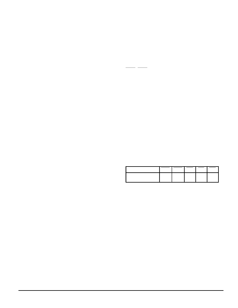
CONTROL PIN TIE VALUES
(H
≥
VIH, L
≤
VIL)
Non–Burst
ADSP
ADSC
ADV
SE1
LBO
Sync Non–Burst,
Pipelined SRAM
H
L
H
L
X
NOTE: Although X is specified in the table as a don’t care, the pin
must be tied either high or low.
相關PDF資料 |
PDF描述 |
|---|---|
| MCM63P636 | 64K x 36 Bit Pipelined BurstRAM Synchronous Fast Static RAM |
| MCM63P736ZP66 | Circular Connector; Body Material:Aluminum; Series:PT07; Number of Contacts:36; Connector Shell Size:22; Connecting Termination:Solder; Circular Shell Style:Jam Nut Receptacle; Circular Contact Gender:Pin; Insert Arrangement:22-36 |
| MCM63P818ZP66 | Circular Connector; No. of Contacts:36; Series:; Body Material:Aluminum; Connecting Termination:Solder; Connector Shell Size:22; Circular Contact Gender:Socket; Circular Shell Style:Jam Nut Receptacle; Insert Arrangement:22-36 |
| MCM63P736ZP100R | Circular Connector; MIL SPEC:MIL-C-26482, Series I, Solder; Body Material:Aluminum; Series:PT07; No. of Contacts:2; Connector Shell Size:8; Connecting Termination:Solder; Circular Shell Style:Jam Nut Receptacle; Body Style:Straight |
| MCM63P818ZP100R | Circular Connector; Body Material:Aluminum; Series:PT07; No. of Contacts:2; Connector Shell Size:8; Connecting Termination:Solder; Circular Shell Style:Jam Nut Receptacle; Circular Contact Gender:Pin; Insert Arrangement:8-2 |
相關代理商/技術參數 |
參數描述 |
|---|---|
| MCM63P631ATQ75 | 制造商:MOTOROLA 制造商全稱:Motorola, Inc 功能描述:64K x 32 Bit Pipelined BurstRAM Synchronous Fast Static RAM |
| MCM63P631ATQ75R | 制造商:MOTOROLA 制造商全稱:Motorola, Inc 功能描述:64K x 32 Bit Pipelined BurstRAM Synchronous Fast Static RAM |
| MCM63P631TQ117 | 制造商:MOTOROLA 制造商全稱:Motorola, Inc 功能描述:64K x 32 Bit Pipelined BurstRAM Synchronous Fast Static RAM |
| MCM63P631TQ117R | 制造商:MOTOROLA 制造商全稱:Motorola, Inc 功能描述:64K x 32 Bit Pipelined BurstRAM Synchronous Fast Static RAM |
| MCM63P631TQ4.5 | 制造商:MOTOROLA 制造商全稱:Motorola, Inc 功能描述:64K x 32 Bit Pipelined BurstRAM Synchronous Fast Static RAM |
發布緊急采購,3分鐘左右您將得到回復。