- 您現在的位置:買賣IC網 > PDF目錄371089 > MCM6706RJ7R2 (MOTOROLA INC) 32K x 8 Bit Static Random Access Memory PDF資料下載
參數資料
| 型號: | MCM6706RJ7R2 |
| 廠商: | MOTOROLA INC |
| 元件分類: | SRAM |
| 英文描述: | 32K x 8 Bit Static Random Access Memory |
| 中文描述: | 32K X 8 STANDARD SRAM, 7 ns, PDSO32 |
| 封裝: | 0.300 INCH, SOJ-32 |
| 文件頁數: | 3/8頁 |
| 文件大小: | 151K |
| 代理商: | MCM6706RJ7R2 |
MCM6706R
3
MOTOROLA FAST SRAM
CAPACITANCE
(f = 1.0 MHz, dV = 3.0 V, TA = 25
°
C, Periodically Sampled Rather Than 100% Tested)
Parameter
Symbol
Max
Unit
Address Input Capacitance
Cin
Cin
Cout
5
pF
Control Pin Input Capacitance (E, G, W)
6
pF
I/O Capacitance
6
pF
AC OPERATING CONDITIONS AND CHARACTERISTICS
(VCC = 5.0 V
±
10%, TA = 0 to + 70
°
C, Unless Otherwise Noted)
Input Timing Measurement Reference Level
Input Pulse Levels
. . . . . . . . . . . . . . . . . . . . . . . . . . . . . . . . .
Input Rise/Fall Time
. . . . . . . . . . . . . . . . . . . . . . . . . . . . . . . . . . . .
1.5 V
. . . . . . . . . . . . . . .
0 to 3.0 V
2 ns
Output Timing Measurement Reference Level
Output Load
. . . . . . . . . . . . . . . . . . . . . . . . . . . . . . . . . .
1.5 V
. . . . . . . . . . . . .
See Figure 1A
READ CYCLE
(See Notes 1 and 2)
MCM6706R–6
MCM6706R–7
MCM6706R–8
Parameter
Symbol
Min
Max
Min
Max
Min
Max
Unit
Notes
Read Cycle Time
tAVAV
tAVQV
tELQV
tGLQV
tAXQX
tELQX
tEHQZ
tGLQX
tGHQZ
6
—
7
—
8
—
ns
3
Address Access Time
—
6
—
7
—
8
ns
Chip Enable Access Time
—
6
—
7
—
8
ns
Output Enable Access Time
—
4
—
4
—
4
ns
Output Hold from Address Change
3
—
3
—
3
—
ns
Chip Enable Low to Output Active
3
—
3
—
3
—
ns
4 ,5, 6
Chip Enable High to Output High–Z
0
3
0
3.5
0
4
ns
4, 5, 6
Output Enable Low to Output Active
0
—
0
—
0
—
ns
4, 5, 6
Output Enable High to Output High–Z
0
3
0
3.5
0
4
ns
4, 5, 6
NOTES:
1. W is high for read cycle.
2. Product sensitivities to noise require proper grounding and decoupling of power supplies as well as minimization or elimination of bus
contention conditions during read and write cycles.
3. All read cycle timing is referenced from the last valid address to the first transitioning address.
4. At any given voltage and temperature, tEHQZ max < tELQX min, and tGHQZ max < tGLQX min, both for a given device and from
device to device.
5. Transition is measured 200 mV from steady–state voltage with load of Figure 1B.
6. This parameter is sampled and not 100% tested.
7. Device is continuously selected (E = VIL, G = VIL).
8. Addresses valid prior to or coincident with E going low.
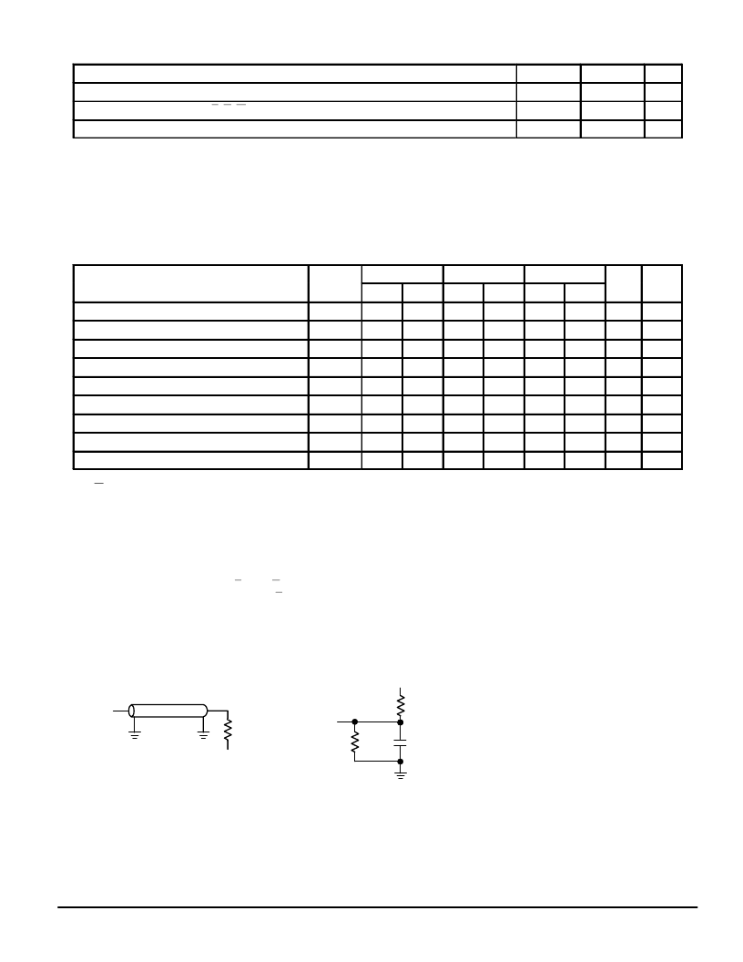
AC TEST LOADS
OUTPUT
Z0 = 50
RL = 50
VL = 1.5 V
Figure 1A
Figure 1B
5 pF
+5 V
OUTPUT
255
480
The table of timing values shows either a
minimum or a maximum limit for each param-
eter. Input requirements are specified from
the external system point of view. Thus, ad-
dress setup time is shown as a minimum
since the system must supply at least that
much time (even though most devices do not
require it). On the other hand, responses from
the memory are specified from the device
point of view. Thus, the access time is shown
as a maximum since the device never pro-
vides data later than that time.
TIMING LIMITS
相關PDF資料 |
PDF描述 |
|---|---|
| MCM6706CRJ5 | 32K x 8 Bit Static Random Access Memory |
| MCM6706CRJ5.5 | 32K x 8 Bit Static Random Access Memory |
| MCM6706CRJ5.5R | 32K x 8 Bit Static Random Access Memory |
| MCM6706CRJ5R | 32K x 8 Bit Static Random Access Memory |
| MCM6708A | 64K x 4 Bit Static RAM |
相關代理商/技術參數 |
參數描述 |
|---|---|
| MCM6706RJ8 | 制造商:MOTOROLA 制造商全稱:Motorola, Inc 功能描述:32K x 8 Bit Static Random Access Memory |
| MCM6706RJ8R2 | 制造商:MOTOROLA 制造商全稱:Motorola, Inc 功能描述:32K x 8 Bit Static Random Access Memory |
| MCM6708A | 制造商:MOTOROLA 制造商全稱:Motorola, Inc 功能描述:64K x 4 Bit Static RAM |
| MCM6708AJ10 | 制造商:MOTOROLA 制造商全稱:Motorola, Inc 功能描述:64K x 4 Bit Static RAM |
| MCM6708AJ10R2 | 制造商:MOTOROLA 制造商全稱:Motorola, Inc 功能描述:64K x 4 Bit Static RAM |
發布緊急采購,3分鐘左右您將得到回復。