- 您現在的位置:買賣IC網 > PDF目錄354436 > MCM69C232TQ20 (MOTOROLA INC) 4K x 64 CAM PDF資料下載
參數資料
| 型號: | MCM69C232TQ20 |
| 廠商: | MOTOROLA INC |
| 元件分類: | DRAM |
| 英文描述: | 4K x 64 CAM |
| 中文描述: | 4K X 64 CONTENT ADDRESSABLE SRAM, 160 ns, PQFP100 |
| 封裝: | TQFP-100 |
| 文件頁數: | 1/16頁 |
| 文件大小: | 175K |
| 代理商: | MCM69C232TQ20 |
MCM69F817
1
MOTOROLA FAST SRAM
Product Preview
256K x 18 Bit Flow–Through
BurstRAM
Synchronous
Fast Static RAM
The MCM69F817 is a 4M bit synchronous fast static RAM designed to provide
a burstable, high performance, secondary cache for the PowerPC
and other
high performance microprocessors. It is organized as 256K words of 18 bits
each. This device integrates input registers, a 2–bit address counter, and high
speed SRAM onto a single monolithic circuit for reduced parts count in cache
data RAM applications. Synchronous design allows precise cycle control with the
use of an external clock (K).
Addresses (SA), data inputs (DQx), and all control signals except output
enable (G) and linear burst order (LBO) are clock (K) controlled through positive–
edge–triggered noninverting registers.
Bursts can be initiated with either ADSP or ADSC input pins. Subsequent burst
addresses can be generated internally by the MCM69F817 (burst sequence
operates in linear or interleaved mode dependent upon the state of LBO) and
controlled by the burst address advance (ADV) input pin.
Write cycles are internally self–timed and are initiated by the rising edge of the
clock (K) input. This feature eliminates complex off–chip write pulse generation
and provides increased timing flexibility for incoming signals.
Synchronous byte write (SBx), synchronous global write (SGW), and synchro-
nous write enable (SW) are provided to allow writes to either individual bytes or
to all bytes. The two bytes are designated as “a” and “b”. SBa controls DQa and
SBb controls DQb. Individual bytes are written if the selected byte writes SBx are
asserted with SW. All bytes are written if either SGW is asserted or if all SBx and
SW are asserted.
For read cycles, a flow–through SRAM allows output data to simply flow freely
from the memory array.
The MCM69F817 operates from a 3.3 V core power supply and all outputs
operate on a 3.3 V or 2.5 V power supply. All inputs and outputs are JEDEC stan-
dard JESD8–5 compatible.
MCM69F817 Speed Options
Speed
tKHKH
Flow–Through
tKHQV
Setup
Hold
IDD
150 MHz
6.7 ns
6 ns
0.5 ns
1 ns
375 mA
133 MHz
7.5 ns
6.5 ns
0.5 ns
1 ns
350 mA
117 MHz
8.5 ns
7 ns
0.5 ns
1 ns
325 mA
3.3 V + 10%, – 5% Core Power Supply, Operates with a 3.3 V or 2.5 V I/O
Supply
ADSP, ADSC, and ADV Burst Control Pins
Selectable Burst Sequencing Order (Linear/Interleaved)
Single–Cycle Deselect Timing
Internally Self–Timed Write Cycle
Byte Write and Global Write Control
PB1 Version 2.0 Compatible
JEDEC Standard 119–Pin PBGA Package
BurstRAM is a trademark of Motorola, Inc.
The PowerPC name is a trademark of IBM Corp., used under license therefrom.
This document contains information on a new product under development. Motorola reserves the right to change or discontinue this product without notice.
Order this document
by MCM69F817/D
MOTOROLA
SEMICONDUCTOR TECHNICAL DATA
MCM69F817
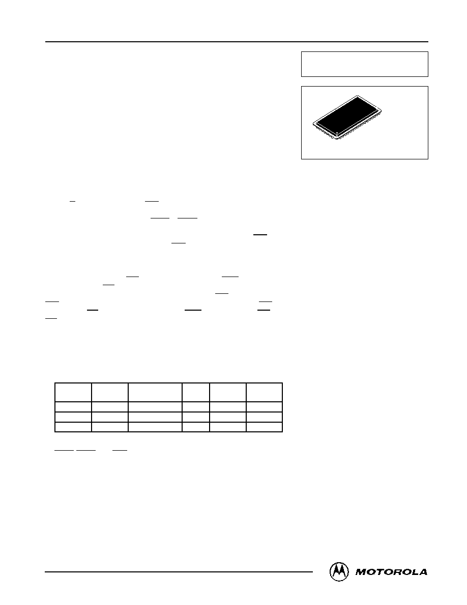
ZP PACKAGE
PBGA
CASE 999–01
REV 1
6/26/97
Motorola, Inc. 1997
相關PDF資料 |
PDF描述 |
|---|---|
| MCM69C232TQ20R | 4K x 64 CAM |
| MCM69C432 | 16K x 64 CAM |
| MCM69C432TQ20 | 16K x 64 CAM |
| MCM69C432TQ20R | 16K x 64 CAM |
| MCM69D536 | 32K x 36 Bit Synchronous Dual I/O, Dual Address SRAM |
相關代理商/技術參數 |
參數描述 |
|---|---|
| MCM69C232TQ20R | 制造商:MOTOROLA 制造商全稱:Motorola, Inc 功能描述:4K x 64 CAM |
| MCM69C233TQ15 | 制造商:Rochester Electronics LLC 功能描述:- Bulk |
| MCM69C233WD | 制造商:MOTOROLA 制造商全稱:Motorola, Inc 功能描述:MPC8260 PowerQUICC II-TM to CAM Interfacing ? MCM69C233 |
| MCM69C233WP | 制造商:MOTOROLA 制造商全稱:Motorola, Inc 功能描述:MPC8260 PowerQUICC II-TM to CAM Interfacing ? MCM69C233 |
| MCM69C432 | 制造商:MOTOROLA 制造商全稱:Motorola, Inc 功能描述:16K x 64 CAM |
發布緊急采購,3分鐘左右您將得到回復。