- 您現在的位置:買賣IC網 > PDF目錄371126 > MMDF3NO2HD (Motorola, Inc.) TMOS DUAL N-CHANNEL FIELD EFFECT TRANSISTOR PDF資料下載
參數資料
| 型號: | MMDF3NO2HD |
| 廠商: | Motorola, Inc. |
| 英文描述: | TMOS DUAL N-CHANNEL FIELD EFFECT TRANSISTOR |
| 中文描述: | TMOS是雙N溝道場效應晶體管 |
| 文件頁數: | 5/10頁 |
| 文件大小: | 188K |
| 代理商: | MMDF3NO2HD |
5
Motorola TMOS Power MOSFET Transistor Device Data
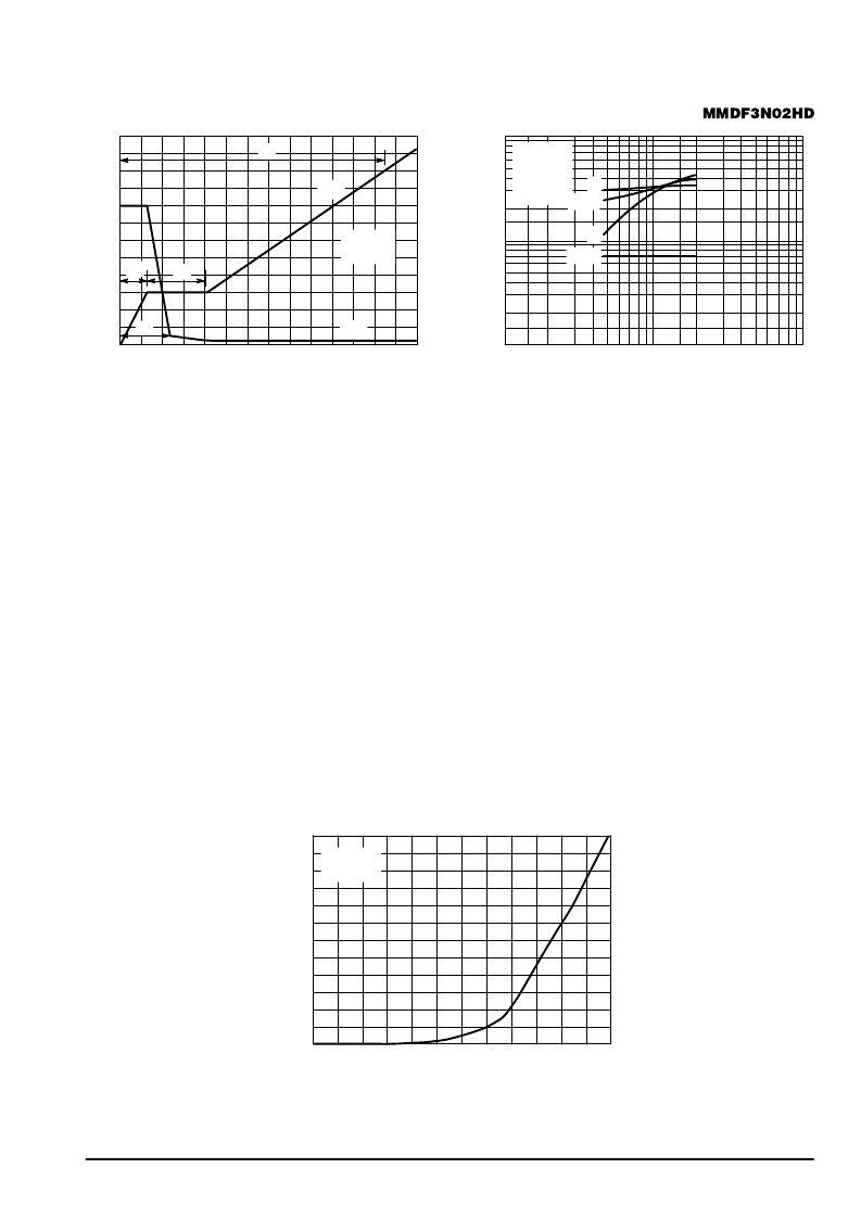
Figure 8. Gate–To–Source and Drain–To–Source
Voltage versus Total Charge
RG, GATE RESISTANCE (OHMS)
1
10
100
100
10
1
t
VDD = 10 V
ID = 3 A
VGS = 10 V
TJ = 25
°
C
tr
tf
td(off)
td(on)
Figure 9. Resistive Switching Time
Variation versus Gate Resistance
24
V
20
16
12
8
4
0
0
10
6
2
0
QT, TOTAL CHARGE (nC)
v
12
8
4
2
4
6
8
14
ID = 3 A
TJ = 25
°
C
10
12
VDS
VGS
QT
Q2
Q3
Q1
DRAIN–TO–SOURCE DIODE CHARACTERISTICS
The switching characteristics of a MOSFET body diode
are very important in systems using it as a freewheeling or
commutating diode. Of particular interest are the reverse re-
covery characteristics which play a major role in determining
switching losses, radiated noise, EMI and RFI.
System switching losses are largely due to the nature of
the body diode itself. The body diode is a minority carrier de-
vice, therefore it has a finite reverse recovery time, trr, due to
the storage of minority carrier charge, QRR, as shown in the
typical reverse recovery wave form of Figure 15. It is this
stored charge that, when cleared from the diode, passes
through a potential and defines an energy loss. Obviously,
repeatedly forcing the diode through reverse recovery further
increases switching losses. Therefore, one would like a
diode with short trr and low QRR specifications to minimize
these losses.
The abruptness of diode reverse recovery effects the
amount of radiated noise, voltage spikes, and current ring-
ing. The mechanisms at work are finite irremovable circuit
parasitic inductances and capacitances acted upon by high
di/dts. The diode’s negative di/dt during ta is directly con-
trolled by the device clearing the stored charge. However,
the positive di/dt during tb is an uncontrollable diode charac-
teristic and is usually the culprit that induces current ringing.
Therefore, when comparing diodes, the ratio of tb/ta serves
as a good indicator of recovery abruptness and thus gives a
comparative estimate of probable noise generated. A ratio of
1 is considered ideal and values less than 0.5 are considered
snappy.
Compared to Motorola standard cell density low voltage
MOSFETs, high cell density MOSFET diodes are faster
(shorter trr), have less stored charge and a softer reverse re-
covery characteristic. The softness advantage of the high
cell density diode means they can be forced through reverse
recovery at a higher di/dt than a standard cell MOSFET
diode without increasing the current ringing or the noise gen-
erated. In addition, power dissipation incurred from switching
the diode will be less due to the shorter recovery time and
lower switching losses.
0.5
0.55
VSD, SOURCE–TO–DRAIN VOLTAGE (VOLTS)
0.6
0.65
0.7
0
1
2
Figure 10. Diode Forward Voltage versus Current
I
1.5
0.75
0.8
0.5
2.5
3
VGS = 0 V
TJ = 25
°
C
相關PDF資料 |
PDF描述 |
|---|---|
| MMDF3N02HD | DUAL TMOS POWER MOSFET 3.0 AMPERES 20 VOLTS |
| MMDF3N03HD | DUAL TMOS POWER MOSFET 4.1 AMPERES 30 VOLTS |
| MMDF3N03HD | Power MOSFET 3 Amps, 30 Volts |
| MMDF3N03HDR2 | Power MOSFET 3 Amps, 30 Volts |
| MMDF4N01HD | DUAL TMOS POWER MOSFET 4.0 AMPERES 20 VOLTS |
相關代理商/技術參數 |
參數描述 |
|---|---|
| MMDF3P03HD | 制造商:MOTOROLA 制造商全稱:Motorola, Inc 功能描述:DUAL TMOS POWER MOSFET 30 VOLTS |
| MMDF4C03HD | 制造商:MOTOROLA 制造商全稱:Motorola, Inc 功能描述:COMPLEMENTARY DUAL TMOS POWER FET 30 VOLTS |
| MMDF4N01HD | 制造商:MOTOROLA 制造商全稱:Motorola, Inc 功能描述:DUAL TMOS POWER MOSFET 4.0 AMPERES 20 VOLTS |
| MMDF4N01HDR2 | 制造商:Rochester Electronics LLC 功能描述:- Bulk 制造商:Motorola Inc 功能描述: 制造商:ON Semiconductor 功能描述: 制造商:MOTOROLA 功能描述: |
| MMDF4P03HD | 制造商:MOTOROLA 制造商全稱:Motorola, Inc 功能描述:DUAL TMOS POWER MOSFET 30 VOLTS |
發布緊急采購,3分鐘左右您將得到回復。