- 您現在的位置:買賣IC網 > PDF目錄371128 > MOC2A6010-5 (Motorola, Inc.) DIODE ZENER 150MW 4.3V 0603 PDF資料下載
參數資料
| 型號: | MOC2A6010-5 |
| 廠商: | Motorola, Inc. |
| 英文描述: | DIODE ZENER 150MW 4.3V 0603 |
| 中文描述: | 光隔離器2安培可控硅過零輸出600伏 |
| 文件頁數: | 1/8頁 |
| 文件大小: | 203K |
| 代理商: | MOC2A6010-5 |
1
Motorola Optoelectronics Device Data
2 Amp Zero–Cross Triac Output
This device consists of a gallium arsenide infrared emitting diode optically
coupled to a zero–cross triac driver circuit and a power triac. It is capable of
driving a load of up to 2 amps (rms) directly, on line voltages from 20 to 280 volts
ac (rms).
Provides Normally Open Solid State AC Output with 2 Amp Rating
70 Amp Single Cycle Surge Capability
Zero–Voltage Turn–on and Zero–Current Turn–off
High Input–Output Isolation of 3750 vac (rms)
Static dv/dt Rating of 400 Volts/
μ
s Guaranteed
2 Amp Pilot Duty Rating Per UL508 117 (Overload Test)
and 118 (Endurance Test)
[File No. 129224]
CSA Approved [File No. CA77170–1].
SEMKO Approved Certificate #9507228
Exceeds NEMA 2–230 and IEEE472 Noise Immunity Test Requirements (See Fig.14)
DEVICE RATINGS
(TA = 25
°
C unless otherwise noted)
Rating
Symbol
Value
Unit
INPUT LED
Forward Current — Maximum Continuous
IF
50
mA
Forward Current — Maximum Peak
(PW = 100
μ
s, 120 pps)
IF(pk)
1.0
A
Reverse Voltage — Maximum
VR
6.0
V
OUTPUT TRIAC
Output Terminal Voltage — Maximum Transient (1)
VDRM
VT
600
V(pk)
Operating Voltage Range — Maximum Continuous
(f = 47 – 63 Hz)
20 to 280
Vac(rms)
On–State Current Range
(Free Air, Power Factor
≥
0.3)
IT(rms)
0.03 to 2.0
A
Non–Repetitive Single Cycle Surge Current —
Maximum Peak (t = 16.7 ms)
ITSM
70
A
Main Terminal Fusing Current (t = 8.3 ms)
I2T
26
A2sec
Load Power Factor Range
PF
0.3 to 1.0
—
Junction Temperature Range
TJ
– 40 to 125
°
C
TOTAL DEVICE
Input–Output Isolation Voltage — Maximum(2)
47 – 63 Hz, 1 sec Duration
VISO
3750
Vac(rms)
Thermal Resistance — Power Triac Junction to Case
(See Fig. 15)
R
θ
JC
8.0
°
C/W
Ambient Operating Temperature Range
Toper
Tstg
TL
– 40 to +100
°
C
°
C
°
C
Storage Temperature Range
– 40 to +150
Lead Soldering Temperature — Maximum
(1/16
″
from Case, 10 sec Duration)
260
1. Test voltages must be applied within dv/dt rating.
2. Input–Output isolation voltage, VISO, is an internal device dielectric breakdown rating. For this
2.
test, pins 2, 3 and the heat tab are common, and pins 7 and 9 are common.
POWER OPTO is a trademark of Motorola, Inc.
Preferred
devices are Motorola recommended choices for future use and best overall value.
Order this document
by MOC2A60–10/D
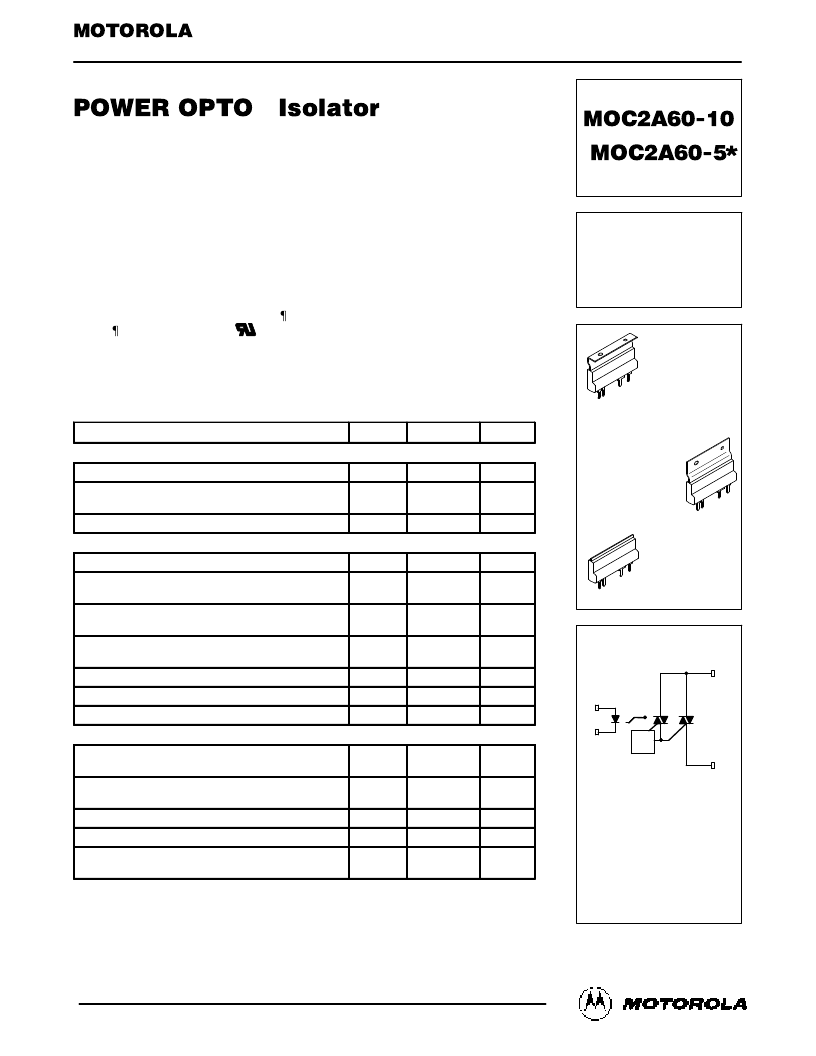
SEMICONDUCTOR TECHNICAL DATA
*Motorola Preferred Device
OPTOISOLATOR
2 AMP ZERO CROSS
TRIAC OUTPUT
600 VOLTS
DEVICE SCHEMATIC
CASE 417–02
Style 2
PLASTIC PACKAGE
CASE 417A–02
Style 1
PLASTIC PACKAGE
CASE 417B–01
Style 1
PLASTIC PACKAGE
23
79
* Zero Voltage Activate Circuit
1, 4, 5, 6, 8. NO PIN
2. LED CATHODE
3. LED ANODE
7. MAIN TERMINAL 2
9. MAIN TERMINAL 1
ZVA
*
7
9
3
2
REV 2
相關PDF資料 |
PDF描述 |
|---|---|
| MOC2R60-10 | OPTOISOLATOR 2 AMPS RANDOM-PHASE TRIAC OUTPUT 600 VOLTS |
| MOC2R60 | OPTOISOLATOR 2 AMPS RANDOM-PHASE TRIAC OUTPUT 600 VOLTS |
| MOC2R60-15 | OPTOISOLATOR 2 AMPS RANDOM-PHASE TRIAC OUTPUT 600 VOLTS |
| MOC2R6010 | OPTOISOLATOR 2 AMPS RANDOM-PHASE TRIAC OUTPUT 600 VOLTS |
| MOC3010 | 6-Pin DIP Random-Phase Optoisolators Triac Driver Output |
相關代理商/技術參數 |
參數描述 |
|---|---|
| MOC2A60-5 | 制造商:Motorola Inc 功能描述: |
| MOC2R60 | 制造商:MOTOROLA 制造商全稱:Motorola, Inc 功能描述:OPTOISOLATOR 2 AMPS RANDOM-PHASE TRIAC OUTPUT 600 VOLTS |
| MOC2R6010 | 制造商:MOTOROLA 制造商全稱:Motorola, Inc 功能描述:OPTOISOLATOR 2 AMPS RANDOM-PHASE TRIAC OUTPUT 600 VOLTS |
| MOC2R60-10 | 制造商:MOTOROLA 制造商全稱:Motorola, Inc 功能描述:OPTOISOLATOR 2 AMPS RANDOM-PHASE TRIAC OUTPUT 600 VOLTS |
| MOC2R60-15 | 制造商:MOTOROLA 制造商全稱:Motorola, Inc 功能描述:OPTOISOLATOR 2 AMPS RANDOM-PHASE TRIAC OUTPUT 600 VOLTS |
發布緊急采購,3分鐘左右您將得到回復。