- 您現(xiàn)在的位置:買賣IC網(wǎng) > PDF目錄26839 > MPC962305EF-1HR2 (FREESCALE SEMICONDUCTOR INC) 962305 SERIES, PLL BASED CLOCK DRIVER, 8 TRUE OUTPUT(S), 0 INVERTED OUTPUT(S), PDSO8 PDF資料下載
參數(shù)資料
| 型號: | MPC962305EF-1HR2 |
| 廠商: | FREESCALE SEMICONDUCTOR INC |
| 元件分類: | 時鐘及定時 |
| 英文描述: | 962305 SERIES, PLL BASED CLOCK DRIVER, 8 TRUE OUTPUT(S), 0 INVERTED OUTPUT(S), PDSO8 |
| 封裝: | 0.150 INCH, SOIC-8 |
| 文件頁數(shù): | 1/6頁 |
| 文件大小: | 110K |
| 代理商: | MPC962305EF-1HR2 |
FREESCALE SEMICONDUCTOR ADVANCED CLOCK DRIVERS DEVICE DATA
507
Freescale Semiconductor, Inc.
TECHNICAL DATA
Order number: MPC962305
Rev 5, 08/2004
Low-Cost 3.3 V Zero Delay Buffer
The MPC962309 is a zero delay buffer designed to distribute high-speed
clocks. Available in a 16-pin SOIC or TSSOP package, the device accepts one
reference input and drives nine low-skew clocks. The MPC962305 is the 8-pin
version of the MPC962309 which drives five outputs with one reference input.
The -1H versions of these devices have higher drive than the -1 devices and
can operate up to 100/-133 MHz frequencies. These parts have on-chip PLLs
which lock to an input clock presented on the REF pin. The PLL feedback is
on-chip and is obtained from the CLOCKOUT pad.
Features
1:5 LVCMOS zero-delay buffer (MPC962305)
1:9 LVCMOS zero-delay buffer (MPC962309)
Zero input-output propagation delay
Multiple low-skew outputs
250 ps max output-output skew
700 ps max device-device skew
Supports a clock I/O frequency range of 10 MHz to 133 MHz,
compatible with CPU and PCI bus frequencies
Low jitter, 200 ps max cycle-cycle, and compatible with Pentium based
systems
Test Mode to bypass PLL (MPC962309 only. See Table 3.Select Input
8-pin SOIC or 8-pin TSSOP package (MPC962305);16-pin SOIC or 16-pin
TSSOP package (MPC962309)
Single 3.3 V supply
Ambient temperature range: –40
°C to +85°C
Compatible with the CY2305, CY23S05, CY2309, CY23S09
Spread spectrum compatible
Functional Description
The MPC962309 has two banks of four outputs each, which can be controlled by the Select Inputs as shown in Table 3.Select Input
Decoding for MPC962309. Bank B can be tri-stated if all of the outputs are not required. Select inputs also allow the input clock to be
directly applied to the outputs for chip and system testing purposes.
The MPC962305 and MPC962309 PLLs enters a power down state when there are no rising edges on the REF input. During this
state, all of the outputs are in tristate, the PLL is turned off, and there is less than 25.0
A of current draw for the device. The PLL
shuts down in one additional case as shown in Table 3.Select Input Decoding for MPC962309.
Multiple MPC962305 and MPC962309 devices can accept the same input clock and distribute it throughout the system. In this
situation, the difference between the output skews of two devices will be less than 700 ps.
All outputs have less than 200 ps of cycle-cycle jitter. The input-to-output propagation delay on both devices is guaranteed to be
less than 350 ps and the output-to-output skew is guaranteed to be less than 250 ps.
The MPC962305 and MPC962309 are available in two/three different configurations, as shown on the ordering information page.
The MPC962305-1/MPC962309-1 are the base parts. High drive versions of those devices, MPC962305-1H and MPC962309-1H,
are available to provide faster rise and fall times of the base device.
Pentium II is a trademark of Intel Corporation.
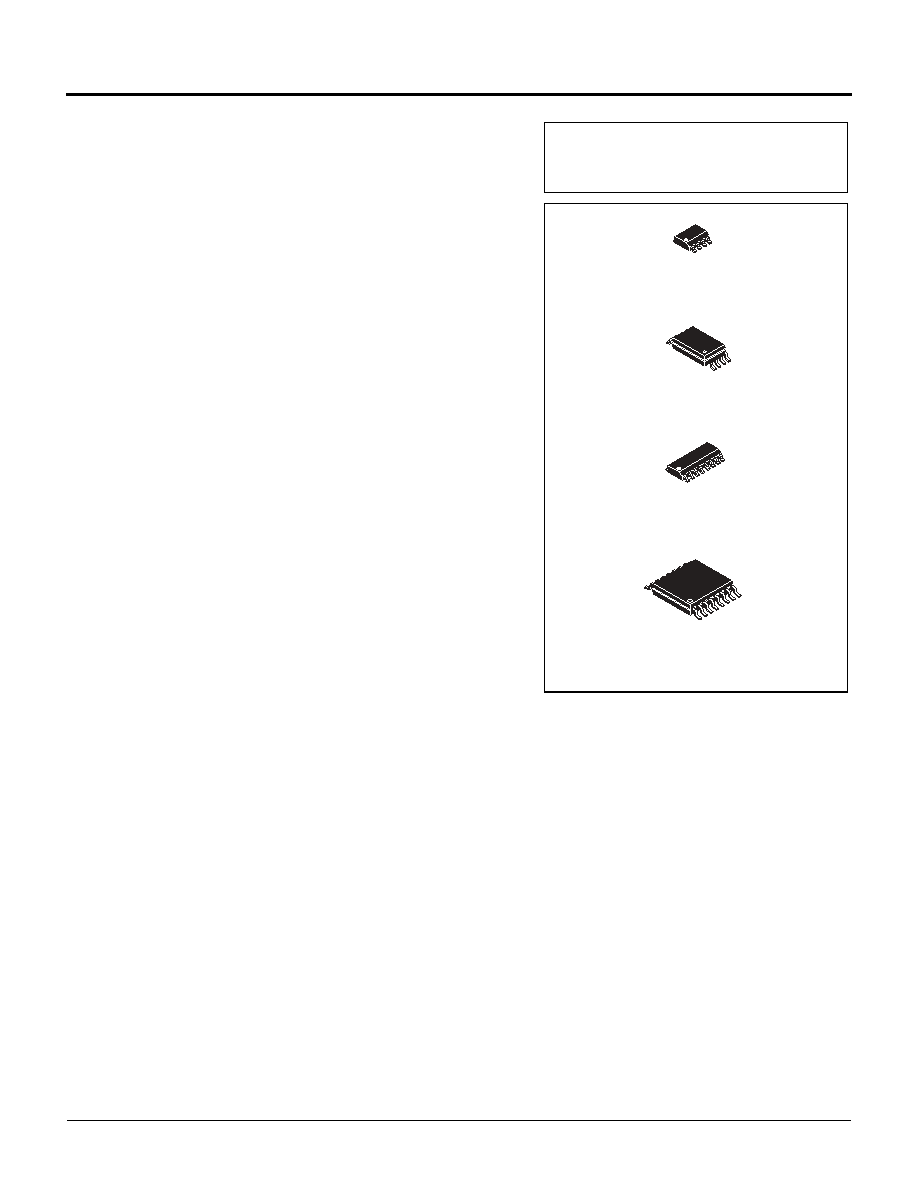
MPC962305
MPC962309
D SUFFIX
16-LEAD SOIC PACKAGE
CASE 751B-05
DT SUFFIX
16-LEAD TSSOP PACKAGE
CASE 948F-01
D SUFFIX
8-LEAD SOIC PACKAGE
CASE 751-06
DT SUFFIX
8-LEAD TSSOP PACKAGE
CASE 948J-01
相關(guān)PDF資料 |
PDF描述 |
|---|---|
| MPC962309EF-1H | 962309 SERIES, PLL BASED CLOCK DRIVER, 8 TRUE OUTPUT(S), 0 INVERTED OUTPUT(S), PDSO16 |
| MPC962305D-1R2 | 962305 SERIES, PLL BASED CLOCK DRIVER, 4 TRUE OUTPUT(S), 0 INVERTED OUTPUT(S), PDSO8 |
| MPC962309EF-1HR2 | 962309 SERIES, PLL BASED CLOCK DRIVER, 8 TRUE OUTPUT(S), 0 INVERTED OUTPUT(S), PDSO16 |
| MPC962305EF-1H | 962305 SERIES, PLL BASED CLOCK DRIVER, 4 TRUE OUTPUT(S), 0 INVERTED OUTPUT(S), PDSO8 |
| MPC962305DT-1H | 962305 SERIES, PLL BASED CLOCK DRIVER, 4 TRUE OUTPUT(S), 0 INVERTED OUTPUT(S), PDSO8 |
相關(guān)代理商/技術(shù)參數(shù) |
參數(shù)描述 |
|---|---|
| MPC962305EF-1R2 | 制造商:IDT 制造商全稱:Integrated Device Technology 功能描述:Low-Cost, 3.3V Zero Delay Buffer |
| MPC962305EJ-1H | 功能描述:時鐘緩沖器 RoHS:否 制造商:Texas Instruments 輸出端數(shù)量:5 最大輸入頻率:40 MHz 傳播延遲(最大值): 電源電壓-最大:3.45 V 電源電壓-最小:2.375 V 最大功率耗散: 最大工作溫度:+ 85 C 最小工作溫度:- 40 C 封裝 / 箱體:LLP-24 封裝:Reel |
| MPC962305EJ-1HR2 | 功能描述:IC BUFFER ZD 1:5 3.3V 8-TSSOP RoHS:是 類別:集成電路 (IC) >> 時鐘/計時 - 時鐘發(fā)生器,PLL,頻率合成器 系列:- 標(biāo)準(zhǔn)包裝:2,000 系列:- 類型:PLL 時鐘發(fā)生器 PLL:帶旁路 輸入:LVCMOS,LVPECL 輸出:LVCMOS 電路數(shù):1 比率 - 輸入:輸出:2:11 差分 - 輸入:輸出:是/無 頻率 - 最大:240MHz 除法器/乘法器:是/無 電源電壓:3.135 V ~ 3.465 V 工作溫度:0°C ~ 70°C 安裝類型:表面貼裝 封裝/外殼:32-LQFP 供應(yīng)商設(shè)備封裝:32-TQFP(7x7) 包裝:帶卷 (TR) |
| MPC962308 | 制造商:MOTOROLA 制造商全稱:Motorola, Inc 功能描述:3.3 V Zero Delay Buffer |
| MPC962308D | 制造商:MOTOROLA 制造商全稱:Motorola, Inc 功能描述:3.3 V Zero Delay Buffer |
發(fā)布緊急采購,3分鐘左右您將得到回復(fù)。