- 您現(xiàn)在的位置:買賣IC網(wǎng) > PDF目錄382350 > MSK3020 (Electronic Theatre Controls, Inc.) H-BRIDGE MOSFET POWER MODULE PDF資料下載
參數(shù)資料
| 型號: | MSK3020 |
| 廠商: | Electronic Theatre Controls, Inc. |
| 英文描述: | H-BRIDGE MOSFET POWER MODULE |
| 中文描述: | H橋MOSFET功率模塊 |
| 文件頁數(shù): | 2/6頁 |
| 文件大小: | 345K |
| 代理商: | MSK3020 |
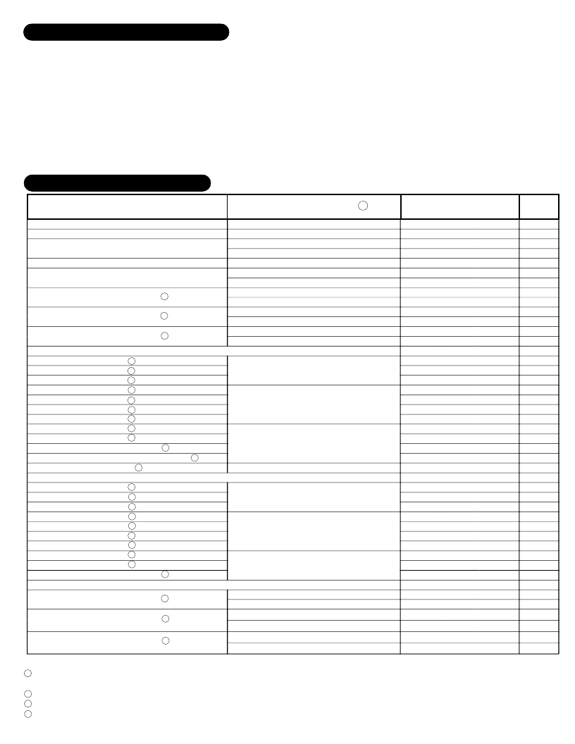
1 This parameter is guaranteed by design but need not be tested. Typical parameters are representative of actual device performance
but are for reference only.
2 Resistance as seen at package pins.
3 Resistance for die only; use for thermal calculations.
4 T
A
= 25°C unless otherwise specified.
NOTES:
V
DSS
V
DGDR
Drain to Source Voltage ........... 100V
Drain to Gate Voltage
(RGS = 1 M
W
)........................ 100V MAX
Gate to Source Voltage
(Continuous)........................... ±20V MAX
Continuous Current .................... 10A MAX
Pulsed Current ........................... 25A MAX
Thermal Resistance
(Junction to Case) .........................4.0°C/W
Sense Current - Continuous ...... 13 mA
MAX
V
GS
I
D
I
DM
R
TH-JC
I
M
MAX
I
MM
MAX
Sense Current Peak ................. 33 mA
2
Rev. A 7/00
ABSOLUTE MAXIMUM RATINGS
Single Pulse Avalanche Energy
(Q1, Q4)........................................................ 7.9 mJ
(Q2, Q3)......................................................... 69 mJ
Junction Temperature............................+175°C MAX
Storage Temperature ........................ -55°C
1
5
Case Operating Temperature Range.... -55°C
1
2
Lead Temperature Range
(10 Seconds)........................................... 300°C MAX
T
J
T
ST
+
T
C
+
T
LD
to
C
to
C
0
°
5
°
Parameter
Test Conditions 4
Drain-Source Breakdown Voltage
Drain-Mirror Breakdown Voltage
Drain-Source Leakage Current
Gate-Source Leakage Current
Gate-Source Threshold Voltage
Drain-Source on Resistance
2
Drain-Source on Resistance
3
Forward Transconductance
1
N-CHANNEL (Q2, Q3)
Total Gate Charge
Gate-Source Charge
Gate-Drain Charge
Turn-On Delay Time
Rise Time
Turn-Off Delay Time 1
Fall Time
Input Capacitance
Output Capacitance
Reverse Transfer Capacitance 1
Output Capacitance of Sensing Cells 1
Current Sensing Ratio 1
P-CHANNEL (Q1, Q4)
Total Gate Charge
Gate-Source Charge
Gate-Drain Charge
Turn-On Delay Time
Rise Time
Turn-Off Delay Time 1
Fall Time
Input Capacitance
Output Capacitance
Reverse Transfer Capacitance 1
BODY DIODE
1
1
1
1
1
1
1
1
1
1
1
1
1
1
1
1
Forward on Voltage
1
Reverse Recovery Time
1
Reverse Recovery Charge
1
I
S
= 14A V
GS
= 0V (Q2, Q3)
I
S
= -14A V
GS
= 0V (Q1, Q4)
I
S
= 14A di/dt = 100A/μS (Q2, Q3)
I
S
= -8.4A di/dt = 100A/μS (Q1, Q4)
I
S
= 14A di/dt = 100A/μS (Q2, Q3)
I
S
= -8.4A di/dt = 100A/μS (Q1, Q4)
V
GS
= 0V
V
DS
= -25V
f = 1 MHz
V
DD
= -50V
I
D
= -8.4A
R
G
= 9.1
W
R
D
= 6.2
W
I
D
= -8.4A
V
DS
= -80V
V
GS
= -10V
V
GS
= 10V I
D
= 14A
V
GS
= 0V
V
DS
= 25V
f = 1 MHz
V
DD
= 50V
I
D
= 14A
R
G
= 12
W
R
D
= 3.5
W
I
D
= 14A
V
DS
= 80V
V
GS
= 10V
V
GS
= 0 I
D
= 0.25 mA (All Transistors)
V
GS
= 0 V
DS
= 100V, (Q2, Q3)
V
DS
= 100V V
GS
= 0V, (Q2, Q3)
V
DS
= -100V V
GS
= 0V, (Q1, Q4)
V
GS
= ±20V V
DS
= 0V (All Transistors)
V
DS
= V
GS
I
D
= 250 μA (Q2, Q3)
V
DS
= V
GS
I
D
= 250 μA (Q1, Q4)
V
GS
= 10V I
D
= 8.4A (Q2, Q3)
V
GS
= -10V I
D
= -8.4A (Q1, Q4)
V
GS
= 10V I
D
= 8.4A (Q2, Q3)
V
GS
= -10V I
D
= -8.4A (Q1, Q4)
V
DS
= 50V I
D
= 8.4A (Q2, Q3)
V
DS
= -50V I
D
= -8.4A (Q1, Q4)
100
100
-
-
-
2.0
-2.0
-
-
-
-
4.7
3.2
-
-
-
-
-
-
-
-
-
-
-
1390
-
-
-
-
-
-
-
-
-
-
-
-
-
-
-
-
9.5
42
22
25
700
320
83
9
-
-
-
25
-25
±100
4.0
-4.0
0.26
0.31
0.16
0.20
-
-
26
5.5
11
-
-
-
-
-
-
-
-
1540
-
-
-
-
-
-
-
-
-
-
-
-
-
-
-
-
2.5
-1.6
150
47
0.85
650
-
-
310
71
1.2
970
V
V
nS
nS
μC
nC
-
-
-
15
58
45
46
760
260
170
58
8.3
32
-
-
-
-
-
-
-
nC
nC
nC
nS
nS
nS
nS
pF
pF
pF
V
V
μA
μA
nA
V
V
W
W
W
W
S
S
nC
nC
nC
nS
nS
nS
nS
pF
pF
pF
pF
r
Units
Typ.
Max.
Min.
MSK 3020
相關PDF資料 |
PDF描述 |
|---|---|
| MSM486SL | The low power, low cost 486 CPU MSM486SL integrates all Functions of a standard PC on one board |
| MSM486SL16 | The low power, low cost 486 CPU MSM486SL integrates all Functions of a standard PC on one board |
| MSM486SL2 | The low power, low cost 486 CPU MSM486SL integrates all Functions of a standard PC on one board |
| MSM486SL8 | The low power, low cost 486 CPU MSM486SL integrates all Functions of a standard PC on one board |
| MSM5105 | MOBILE STATION MODEM, 3G CDMA Enabling Chipset (Pin compatible with the MSM3100 in a 208 FBGA package) |
相關代理商/技術參數(shù) |
參數(shù)描述 |
|---|---|
| MSK35 | 制造商:Marathon Special Products 功能描述:END BRACKET SECTIONAL TERMINAL BLOCK 制造商:MARATHON 功能描述:END BRACKET, SECTIONAL TERMINAL BLOCK 制造商:MARATHON 功能描述:END BRACKET, SECTIONAL TERMINAL BLOCK; Series:MIK 5; Accessory Type:End Bracket; For Use With:Sectional Terminal Blocks; Body Material:Polyamide; Color:Gray; Current Rating:40A; Depth:6mm; Height:38mm; Line Wire Range:#22-#10 AWG ;RoHS Compliant: Yes 制造商:Marathon Special Products 功能描述:Terminal Block |
| MSK3554 | 制造商:未知廠家 制造商全稱:未知廠家 功能描述:HIGH SPEED, WIDEBAND OPERATIONAL AMPLIFIER |
| MSK3554B | 制造商:未知廠家 制造商全稱:未知廠家 功能描述:HIGH SPEED, WIDEBAND OPERATIONAL AMPLIFIER |
| MSK35W | 制造商:Marathon Special Products 功能描述: |
| MSK4200 | 制造商:MSK 制造商全稱:M.S. Kennedy Corporation 功能描述:75 VOLT 5 AMP MOSFET H-BRIDGE PWM MOTOR DRIVER/AMPLIFIER |
發(fā)布緊急采購,3分鐘左右您將得到回復。