- 您現在的位置:買賣IC網 > PDF目錄371151 > MTD1N80E (MOTOROLA INC) TMOS POWER FET 1.0 AMPERES 800 VOLTS RDS(on) = 12 OHM PDF資料下載
參數資料
| 型號: | MTD1N80E |
| 廠商: | MOTOROLA INC |
| 元件分類: | JFETs |
| 英文描述: | TMOS POWER FET 1.0 AMPERES 800 VOLTS RDS(on) = 12 OHM |
| 中文描述: | 1 A, 800 V, 12 ohm, N-CHANNEL, Si, POWER, MOSFET |
| 文件頁數: | 1/10頁 |
| 文件大小: | 269K |
| 代理商: | MTD1N80E |
1
Motorola, Inc. 1995
!
N–Channel Enhancement–Mode Silicon Gate
This high voltage MOSFET uses an advanced termination
scheme to provide enhanced voltage–blocking capability without
degrading performance over time. In addition this advanced TMOS
E–FET is designed to withstand high energy in the avalanche and
commutation modes. The new energy efficient design also offers a
drain–to–source diode with a fast recovery time. Designed for high
voltage, high speed switching applications in power supplies,
converters and PWM motor controls, these devices are particularly
well suited for bridge circuits where diode speed and commutating
safe operating areas are critical and offer additional safety margin
against unexpected voltage transients.
Robust High Voltage Termination
Avalanche Energy Specified
Source–to–Drain Diode Recovery Time Comparable to a Discrete
Fast Recovery Diode
Diode is Characterized for Use in Bridge Circuits
IDSS and VDS(on) Specified at Elevated Temperature
Surface Mount Package Available in 16 mm, 13–inch/2500
Unit Tape & Reel, Add T4 Suffix to Part Number
MAXIMUM RATINGS
(TC = 25
°
C unless otherwise noted)
Rating
Symbol
Value
Unit
Drain–to–Source Voltage
VDSS
VDGR
VGS
VGSM
800
Vdc
Drain–to–Gate Voltage (RGS = 1.0 M
)
Gate–to–Source Voltage — Continuous
Gate–to–Source Voltage
— Non–Repetitive (tp
≤
10 ms)
800
Vdc
±
20
±
40
Vdc
Vpk
Drain Current — Continuous
Drain Current
— Continuous @ 100
°
C
Drain Current
— Single Pulse (tp
≤
10
μ
s)
ID
ID
IDM
1.0
0.8
3.0
Adc
Apk
Total Power Dissipation
Derate above 25
°
C
Total Power Dissipation @ TA = 25
°
C, when mounted to minimum recommended pad size
PD
48
0.38
1.75
Watts
W/
°
C
Watts
Operating and Storage Temperature Range
TJ, Tstg
EAS
–55 to 150
°
C
Single Pulse Drain–to–Source Avalanche Energy — Starting TJ = 25
°
C
(VDD = 100 Vdc, VGS = 10 Vdc, IL = 2.0 Apk, L = 10 mH, RG = 25
)
20
mJ
Thermal Resistance — Junction to Case
Thermal Resistance
— Junction to Ambient
Thermal Resistance
— Junction to Ambient, when mounted to minimum recommended pad size
R
θ
JC
R
θ
JA
R
θ
JA
TL
2.6
100
71.4
°
C/W
Maximum Temperature for Soldering Purposes, 1/8
″
from case for 10 seconds
260
°
C
Designer’s Data for “Worst Case” Conditions
— The Designer’s Data Sheet permits the design of most circuits entirely from the information presented. SOA Limit
curves — representing boundaries on device characteristics — are given to facilitate “worst case” design.
E–FET and Designer’s are trademarks of Motorola, Inc. TMOS is a registered trademark of Motorola, Inc.
Thermal Clad is a trademark of the Bergquist Company.
Preferred
devices are Motorola recommended choices for future use and best overall value.
REV 1
SEMICONDUCTOR TECHNICAL DATA
Order this document
by MTD1N80E/D
TMOS POWER FET
1.0 AMPERES
800 VOLTS
RDS(on) = 12 OHM
Motorola Preferred Device
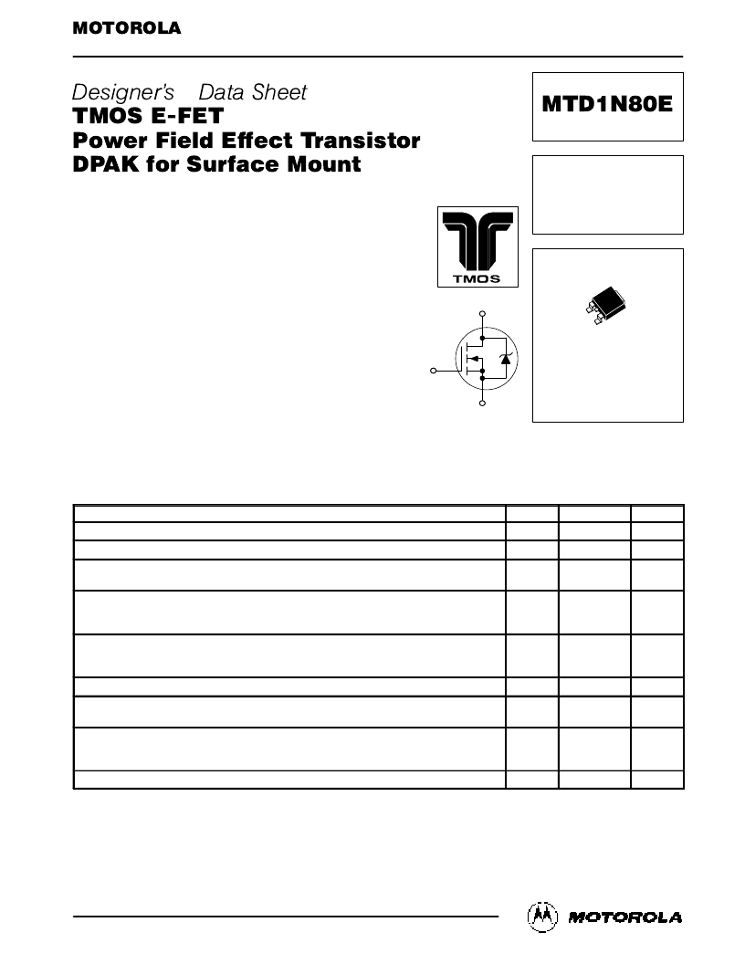
D
S
G
CASE 369A–13, Style 2
DPAK
相關PDF資料 |
PDF描述 |
|---|---|
| MTD20N06HD | TMOS POWER FET 20 AMPERES 60 VOLTS RDS(on) = 0.045 OHM |
| MTD20N06HDL | TMOS POWER FET LOGIC LEVEL 20 AMPERES 60 VOLTS RDS(on) = 0.045 OHM |
| MTD20P03 | TMOS POWER FET LOGIC LEVEL 19 AMPERES 30 VOLTS RDS(on) = 0.099 OHM |
| MTD20N06 | TMOS POWER FET 20 AMPERES 60 VOLTS RDS(on) = 0.080 OHM |
| MTD20P06 | TMOS POWER FET LOGIC LEVEL 15 AMPERES 60 VOLTS RDS(on) = 175 MOHM |
相關代理商/技術參數 |
參數描述 |
|---|---|
| MTD1P40ET4 | 制造商:Rochester Electronics LLC 功能描述:- Bulk |
| MTD1P50E | 制造商:MOTOROLA 制造商全稱:Motorola, Inc 功能描述:TMOS POWER FET 1.0 AMPERES 500 VOLTS 15 OHM |
| MTD2001 | 制造商:SHINDENGEN 制造商全稱:Shindengen Electric Mfg.Co.Ltd 功能描述:Stepping Motor Driver ICs |
| MTD2001-4101 | 功能描述:馬達/運動/點火控制器和驅動器 VCEO=60 IO=1.5 PT=5 RoHS:否 制造商:STMicroelectronics 產品:Stepper Motor Controllers / Drivers 類型:2 Phase Stepper Motor Driver 工作電源電壓:8 V to 45 V 電源電流:0.5 mA 工作溫度:- 25 C to + 125 C 安裝風格:SMD/SMT 封裝 / 箱體:HTSSOP-28 封裝:Tube |
| MTD2001-4102 | 功能描述:馬達/運動/點火控制器和驅動器 VCEO=60 IO=1.5 PT=5 RoHS:否 制造商:STMicroelectronics 產品:Stepper Motor Controllers / Drivers 類型:2 Phase Stepper Motor Driver 工作電源電壓:8 V to 45 V 電源電流:0.5 mA 工作溫度:- 25 C to + 125 C 安裝風格:SMD/SMT 封裝 / 箱體:HTSSOP-28 封裝:Tube |
發布緊急采購,3分鐘左右您將得到回復。