- 您現在的位置:買賣IC網 > PDF目錄383646 > MTD2955V-1 (ON SEMICONDUCTOR) 30V N-Channel PowerTrench MOSFET PDF資料下載
參數資料
| 型號: | MTD2955V-1 |
| 廠商: | ON SEMICONDUCTOR |
| 元件分類: | 功率晶體管 |
| 英文描述: | 30V N-Channel PowerTrench MOSFET |
| 中文描述: | 12 A, 60 V, 0.23 ohm, P-CHANNEL, Si, POWER, MOSFET |
| 封裝: | CASE 369D-01, DPAK-3 |
| 文件頁數: | 1/10頁 |
| 文件大小: | 85K |
| 代理商: | MTD2955V-1 |
Semiconductor Components Industries, LLC, 2004
April, 2004 Rev. 7
1
Publication Order Number:
MTD2955V/D
MTD2955V
Power MOSFET 12 A, 60 V
PChannel DPAK
This Power MOSFET is designed to withstand high energy in the
avalanche and commutation modes. Designed for low voltage, high
speed switching applications in power supplies, converters and power
motor controls, these devices are particularly well suited for bridge
circuits where diode speed and commutating safe operating areas are
critical and offer additional safety margin against unexpected voltage
transients.
Features
Avalanche Energy Specified
I
DSS
and V
DS(on)
Specified at Elevated Temperature
PbFree Packages are Available
MAXIMUM RATINGS
(T
C
= 25
°
C unless otherwise noted)
Rating
Symbol
Value
Unit
DraintoSource Voltage
V
DSS
V
DGR
60
Vdc
DraintoGate Voltage (R
GS
= 1.0 M )
GatetoSource Voltage
Continuous
Nonrepetitive (t
p
≤
10 ms)
Drain Current Continuous
Drain Current
Continuous @ 100
°
C
Drain Current
Single Pulse (t
p
≤
10 s)
Total Power Dissipation
Derate above 25
°
C
Total Power Dissipation @ 25
°
C (Note 2)
60
Vdc
V
GS
V
GSM
I
D
I
D
I
DM
P
D
±
20
±
25
Vdc
Vpk
12
8.0
42
Adc
Apk
60
0.4
2.1
Watts
W/
°
C
Watts
Operating and Storage Temperature
Range
T
J
, T
stg
55 to
175
°
C
Single Pulse DraintoSource Avalanche
Energy Starting T
J
= 25
°
C
(V
DD
= 25 Vdc, V
GS
= 10 Vdc, Peak
I
L
= 12 Apk, L = 3.0 mH, R
G
= 25 )
Thermal Resistance
Junction to Case
Junction to Ambient (Note 1)
Junction to Ambient (Note 2)
E
AS
216
mJ
R
JC
R
JA
R
JA
T
L
2.5
100
71.4
°
C/W
Maximum Lead Temperature for Soldering
Purposes, 1/8
″
from case for 10
seconds
260
°
C
Maximum ratings are those values beyond which device damage can occur.
Maximum ratings applied to the device are individual stress limit values (not
normal operating conditions) and are not valid simultaneously. If these limits
are exceeded, device functional operation is not implied, damage may occur
and reliability may be affected.
1. When surface mounted to an FR4 board using the minimum recommended
pad size.
2. When surface mounted to an FR4 board using the 0.5 sq.in. pad size.
D
S
G
12 A, 60 V
R
DS(on)
= 185 m (Typ)
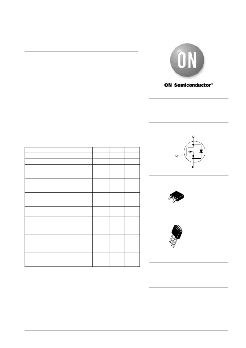
PChannel
http://onsemi.com
DPAK3
CASE 369C
STYLE 2
1 2
3
4
DPAK3
CASE 369D
STYLE 2
123
4
See detailed ordering and shipping information in the
package dimensions section on page 7 of this data sheet.
ORDERING INFORMATION
See general marking information in the device marking
section on page 7 of this data sheet.
DEVICE MARKING INFORMATION
相關PDF資料 |
PDF描述 |
|---|---|
| MTD2955V-1G | 30V N-Channel PowerTrench MOSFET |
| MTD2955VG | 30V N-Channel PowerTrench MOSFET |
| MTD2955VT4 | 30V N-Channel PowerTrench MOSFET |
| MTD2955VT4G | 30V N-Channel PowerTrench MOSFET |
| MTP | Wet Tantalum Capacitors Subminiature, Axial Leads |
相關代理商/技術參數 |
參數描述 |
|---|---|
| MTD2955V-1G | 制造商:ONSEMI 制造商全稱:ON Semiconductor 功能描述:Power MOSFET 12A, 60V P-Channel DPAK |
| MTD2955VG | 制造商:ONSEMI 制造商全稱:ON Semiconductor 功能描述:Power MOSFET 12A, 60V P-Channel DPAK |
| MTD2955VT4 | 功能描述:MOSFET P-CH 60V 12A DPAK RoHS:否 類別:分離式半導體產品 >> FET - 單 系列:- 標準包裝:1,000 系列:MESH OVERLAY™ FET 型:MOSFET N 通道,金屬氧化物 FET 特點:邏輯電平門 漏極至源極電壓(Vdss):200V 電流 - 連續漏極(Id) @ 25° C:18A 開態Rds(最大)@ Id, Vgs @ 25° C:180 毫歐 @ 9A,10V Id 時的 Vgs(th)(最大):4V @ 250µA 閘電荷(Qg) @ Vgs:72nC @ 10V 輸入電容 (Ciss) @ Vds:1560pF @ 25V 功率 - 最大:40W 安裝類型:通孔 封裝/外殼:TO-220-3 整包 供應商設備封裝:TO-220FP 包裝:管件 |
| MTD2955VT4G | 制造商:ONSEMI 制造商全稱:ON Semiconductor 功能描述:Power MOSFET 12A, 60V P-Channel DPAK |
| MTD2N20 | 制造商:MOTOROLA 制造商全稱:Motorola, Inc 功能描述:POWER FIELD EFFECT TRANSISTOR N-CHANNEL ENHANCEMENT-MODE SILICON GATE |
發布緊急采購,3分鐘左右您將得到回復。