- 您現(xiàn)在的位置:買賣IC網(wǎng) > PDF目錄371152 > MTP2N60 (MOTOROLA INC) TMOS POWER FET 2.0 AMPERES 600 VOLTS RDS(on) = 3.8 OHMS PDF資料下載
參數(shù)資料
| 型號: | MTP2N60 |
| 廠商: | MOTOROLA INC |
| 元件分類: | JFETs |
| 英文描述: | TMOS POWER FET 2.0 AMPERES 600 VOLTS RDS(on) = 3.8 OHMS |
| 中文描述: | 2 A, 600 V, 6 ohm, N-CHANNEL, Si, POWER, MOSFET, TO-220AB |
| 文件頁數(shù): | 1/8頁 |
| 文件大小: | 219K |
| 代理商: | MTP2N60 |
1
Motorola, Inc. 1996
N–Channel Enhancement–Mode Silicon Gate
This high voltage MOSFET uses an advanced termination
scheme to provide enhanced voltage–blocking capability without
degrading performance over time. In addition, this advanced TMOS
E–FET is designed to withstand high energy in the avalanche and
commutation modes. The new energy efficient design also offers a
drain–to–source diode with a fast recovery time. Designed for high
voltage, high speed switching applications in power supplies,
converters and PWM motor controls, these devices are particularly
well suited for bridge circuits where diode speed and commutating
safe operating areas are critical and offer additional safety margin
against unexpected voltage transients.
Robust High Voltage Termination
Avalanche Energy Specified
Source–to–Drain Diode Recovery Time Comparable to a Discrete
Fast Recovery Diode
Diode is Characterized for Use in Bridge Circuits
IDSS and VDS(on) Specified at Elevated Temperature
MAXIMUM RATINGS
(TC = 25
°
C unless otherwise noted)
Rating
Symbol
Value
Unit
Drain–to–Source Voltage
VDSS
VDGR
VGS
600
Vdc
Drain–to–Gate Voltage (RGS = 1.0 M
)
Gate–to–Source Voltage — Continuous
600
Vdc
— Single Pulse (tp
≤
50
μ
s)
±
20
±
40
Vdc
Drain Current — Continuous
— Single Pulse (tp
≤
10
μ
s)
ID
IDM
2.0
9.0
Adc
Total Power Dissipation
Derate above 25
°
C
PD
50
0.4
Watts
W/
°
C
Operating and Storage Temperature Range
TJ, Tstg
EAS
–55 to 150
°
C
Single Pulse Drain–to–Source Avalanche Energy — Starting TJ = 25
°
C
(VDD = 50 Vdc, VGS = 10 Vdc, L = 95 mH, RG = 25
, Peak IL = 2.0 Adc)
190
mJ
Thermal Resistance — Junction to Case
°
— Junction to Ambient
°
R
θ
JC
R
θ
JA
TL
2.5
°
62.5
°
°
C/W
Maximum Lead Temperature for Soldering Purposes, 1/8
″
from case for 10 seconds
260
°
C
Designer’s Data for “Worst Case” Conditions
— The Designer’s Data Sheet permits the design of most circuits entirely from the information presented. SOA Limit
curves — representing boundaries on device characteristics — are given to facilitate “worst case” design.
E–FET and Designer’s are trademarks of Motorola, Inc. TMOS is a registered trademark of Motorola, Inc.
Preferred
devices are Motorola recommended choices for future use and best overall value.
REV 2
Order this document
by MTP2N60E/D
SEMICONDUCTOR TECHNICAL DATA
TMOS POWER FET
2.0 AMPERES
600 VOLTS
RDS(on) = 3.8 OHMS
Motorola Preferred Device
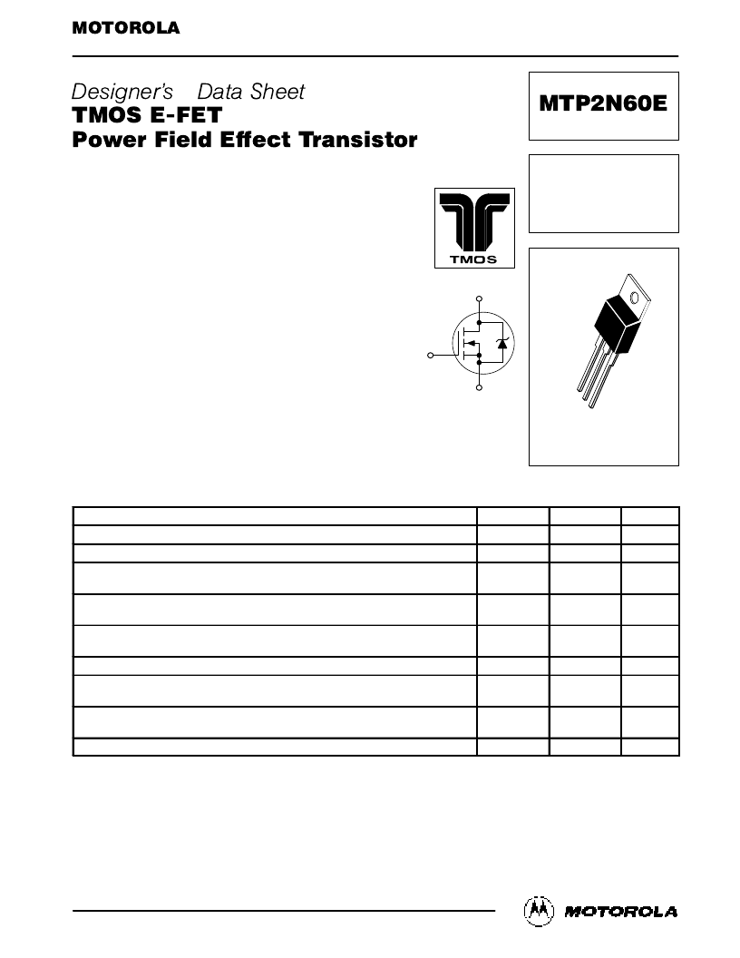
D
S
G
CASE 221A–06, Style 5
TO–220AB
相關(guān)PDF資料 |
PDF描述 |
|---|---|
| MTP2N60E | TMOS POWER FET 2.0 AMPERES 600 VOLTS RDS(on) = 3.8 OHMS |
| MTP2P50E | TMOS POWER FET 2.0 AMPERES 500 VOLTS RDS(on) = 6.0 OHM |
| MTP2P50 | TMOS POWER FET 2.0 AMPERES 500 VOLTS RDS(on) = 6.0 OHM |
| MTP3055 | TMOS POWER FET 12 AMPERES 60 VOLTS RDS(on) = 0.15 OHM |
| MTP3055 | N - CHANNEL 60V - 0.1ohm - 12A TO-220 STripFET MOSFET |
相關(guān)代理商/技術(shù)參數(shù) |
參數(shù)描述 |
|---|---|
| MTP2N60E | 制造商:MOTOROLA 制造商全稱:Motorola, Inc 功能描述:TMOS POWER FET 2.0 AMPERES 600 VOLTS RDS(on) = 3.8 OHMS |
| MTP2P50 | 制造商:MOTOROLA 制造商全稱:Motorola, Inc 功能描述:TMOS POWER FET 2.0 AMPERES 500 VOLTS RDS(on) = 6.0 OHM |
| MTP2P50E | 功能描述:MOSFET 500V 2A P-Channel RoHS:否 制造商:STMicroelectronics 晶體管極性:N-Channel 汲極/源極擊穿電壓:650 V 閘/源擊穿電壓:25 V 漏極連續(xù)電流:130 A 電阻汲極/源極 RDS(導通):0.014 Ohms 配置:Single 最大工作溫度: 安裝風格:Through Hole 封裝 / 箱體:Max247 封裝:Tube |
| MTP2P50E_10 | 制造商:ONSEMI 制造商全稱:ON Semiconductor 功能描述:Power MOSFET 2 Amps, 500 Volts |
| MTP2P50EG | 功能描述:MOSFET 500V 2A P-Channel RoHS:否 制造商:STMicroelectronics 晶體管極性:N-Channel 汲極/源極擊穿電壓:650 V 閘/源擊穿電壓:25 V 漏極連續(xù)電流:130 A 電阻汲極/源極 RDS(導通):0.014 Ohms 配置:Single 最大工作溫度: 安裝風格:Through Hole 封裝 / 箱體:Max247 封裝:Tube |
發(fā)布緊急采購,3分鐘左右您將得到回復。