- 您現在的位置:買賣IC網 > PDF目錄16726 > NB3N3020DTGEVB (ON Semiconductor)BOARD EVAL NB3N3020 CLOCK MULT PDF資料下載
參數資料
| 型號: | NB3N3020DTGEVB |
| 廠商: | ON Semiconductor |
| 文件頁數: | 5/9頁 |
| 文件大小: | 0K |
| 描述: | BOARD EVAL NB3N3020 CLOCK MULT |
| 標準包裝: | 1 |
| 主要目的: | 計時,時鐘乘法器 |
| 嵌入式: | 否 |
| 已用 IC / 零件: | NB3N3020 |
| 主要屬性: | 1 輸入,2 輸出 |
| 次要屬性: | SMA 連接器 |
| 已供物品: | 板 |
| 其它名稱: | NB3N3020DTGEVB-ND NB3N3020DTGEVBOS |
NB3N3020
http://onsemi.com
5
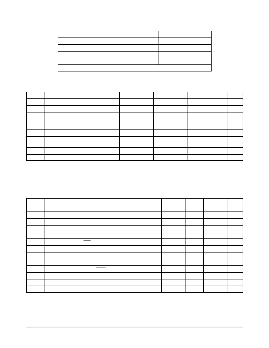
Table 3. ATTRIBUTES
Characteristics
Value
ESD Protection
Human Body Model
2 kV
Moisture Sensitivity, Indefinite Time Out of Dry pack (Note 1)
Level 1
Flammability Rating
Oxygen Index: 28 to 34
UL 94 V0 @ 0.125 in
Transistor Count
8287 Devices
Meets or exceeds JEDEC Spec EIA/JESD78 IC Latchup Test
1. For additional information, see Application Note AND8003/D.
Table 4. MAXIMUM RATINGS (Note 2)
Symbol
Parameter
Condition 1
Condition 2
Rating
Unit
VDD
Positive Power Supply
GND = 0 V
4.6
V
VI
Input Voltage (VIN)
GND = 0 V
GND ≤ VI ≤ VDD
0.5 V to VDD + 0.5 V
V
Iout
LVPECL Output Current
Continuous
Surge
25
50
mA
TA
Operating Temperature Range
40 to +85
°C
Tstg
Storage Temperature Range
65 to +150
°C
qJA
Thermal Resistance (JunctiontoAmbient)
0 lfpm
500 lfpm
TSSOP–16
138
108
°C/W
qJC
Thermal Resistance (JunctiontoCase)
(Note 3)
TSSOP16
33 to 36
°C/W
Tsol
Wave Solder
265
°C
Stresses exceeding Maximum Ratings may damage the device. Maximum Ratings are stress ratings only. Functional operation above the
Recommended Operating Conditions is not implied. Extended exposure to stresses above the Recommended Operating Conditions may affect
device reliability.
2. Maximum ratings applied to the device are individual stress limit values (not normal operating conditions) and not valid simultaneously. If
stress limits are exceeded device functional operation is not implied, damage may occur and reliability may be affected.
3. JEDEC standard multilayer board 2S2P (2 signal, 2 power).
Table 5. DC CHARACTERISTICS (VDD = 3.3 V ±10%, GND = 0 V, TA = 40°C to +85°C)
Symbol
Characteristic
Min
Typ
Max
Unit
VDD
Power Supply Voltage
2.97
3.3
3.63
V
IDD
Power Supply Current (Note 4)
60
75
mA
IDDOE
Power Supply Current when OE1, OE2 is Set Low
50
mA
IDDOFF
Power Supply Current when PLL is powered off by Sel0, Sel1, Sel2
5
mA
VIH
Input HIGH Voltage (X1/CLK, OE1, OE2)
2000
VDD + 300
mV
VIL
Input LOW Voltage (X1/CLK, OE1, OE2)
GND 300
800
mV
VIH
Input HIGH Voltage (Sel0, Sel1, Sel2)
0.72 VDD
VDD + 300
mV
VIL
Input LOW Voltage (Sel0, Sel1, Sel2)
GND 300
800
mV
VIM
Input Mid Voltage (Sel0, Sel1, Sel2) (When left open, defaults to VDD/2
VDD/2
mV
VOH
Output HIGH Voltage for CLK2, CLK2 (See Figure 3)
VDD – 1.145
VDD – 0.895
V
VOL
Output LOW Voltage for CLK2, CLK2 (See Figure 3)
VDD – 2.090
VDD – 1.600
V
VOH
Output HIGH Voltage for CLK1 [IOH = 12 mA]
2.4
V
VOL
Output LOW Voltage for CLK1 [IOL = 12 mA]
0.4
V
NOTE: Device will meet the specifications after thermal equilibrium has been established when mounted in a test socket or printed circuit
board with maintained transverse airflow greater than 500 lfpm. Electrical parameters are guaranteed only over the declared
operating temperature range. Functional operation of the device exceeding these conditions is not implied. Device specification limit
values are applied individually under normal operating conditions and not valid simultaneously.
4. Measurement taken at FCLKout = 125 MHz with LVPECL and LVCMOS/ LVTTL outputs not terminated.
相關PDF資料 |
PDF描述 |
|---|---|
| NB7L216MNEVB | EVAL BOARD FOR NB7L216MN |
| H3CWH-1006M | IDC CABLE - HKC10H/AE10M/HPL10H |
| RBC18DRYH | CONN EDGECARD 36POS DIP .100 SLD |
| RBC07DREH-S93 | CONN EDGECARD 14POS .100 EYELET |
| MAX6102EUR-T | IC VREF SERIES 2.5V SOT-23-3 |
相關代理商/技術參數 |
參數描述 |
|---|---|
| NB3N3020DTR2G | 功能描述:鎖相環 - PLL LVPECL CLK MULTIPLR 3.3V RoHS:否 制造商:Silicon Labs 類型:PLL Clock Multiplier 電路數量:1 最大輸入頻率:710 MHz 最小輸入頻率:0.002 MHz 輸出頻率范圍:0.002 MHz to 808 MHz 電源電壓-最大:3.63 V 電源電壓-最小:1.71 V 最大工作溫度:+ 85 C 最小工作溫度:- 40 C 封裝 / 箱體:QFN-36 封裝:Tray |
| NB3N49152MNG | 功能描述:時鐘發生器及支持產品 VCXO LVPECL 491.52 MHZ RoHS:否 制造商:Silicon Labs 類型:Clock Generators 最大輸入頻率:14.318 MHz 最大輸出頻率:166 MHz 輸出端數量:16 占空比 - 最大:55 % 工作電源電壓:3.3 V 工作電源電流:1 mA 最大工作溫度:+ 85 C 安裝風格:SMD/SMT 封裝 / 箱體:QFN-56 |
| NB3N49152MNTXG | 功能描述:時鐘發生器及支持產品 VCXO LVPECL 491.52 MHZ RoHS:否 制造商:Silicon Labs 類型:Clock Generators 最大輸入頻率:14.318 MHz 最大輸出頻率:166 MHz 輸出端數量:16 占空比 - 最大:55 % 工作電源電壓:3.3 V 工作電源電流:1 mA 最大工作溫度:+ 85 C 安裝風格:SMD/SMT 封裝 / 箱體:QFN-56 |
| NB3N501 | 制造商:ONSEMI 制造商全稱:ON Semiconductor 功能描述:3.3V / 5.0V 13 MHz to 160 MHz PLL Clock Multiplier |
| NB3N501DG | 功能描述:時鐘緩沖器 PLL CLOCK MULTIPLIER RoHS:否 制造商:Texas Instruments 輸出端數量:5 最大輸入頻率:40 MHz 傳播延遲(最大值): 電源電壓-最大:3.45 V 電源電壓-最小:2.375 V 最大功率耗散: 最大工作溫度:+ 85 C 最小工作溫度:- 40 C 封裝 / 箱體:LLP-24 封裝:Reel |
發布緊急采購,3分鐘左右您將得到回復。