參數資料
| 型號: | NB4L16MMNR2G |
| 廠商: | ON Semiconductor |
| 文件頁數: | 1/12頁 |
| 文件大小: | 0K |
| 描述: | IC CLK BUFFER DVR TRANSLA 16-QFN |
| 標準包裝: | 3,000 |
| 類型: | 緩沖器/驅動器,變換器 |
| 電路數: | 1 |
| 比率 - 輸入:輸出: | 2:1 |
| 差分 - 輸入:輸出: | 是/是 |
| 輸入: | CML,HSTL,LVCMOS,LVDS,LVPECL,LVTTL |
| 輸出: | CML |
| 頻率 - 最大: | 3.5GHz |
| 電源電壓: | 2.375 V ~ 3.8 V |
| 工作溫度: | -40°C ~ 85°C |
| 安裝類型: | 表面貼裝 |
| 封裝/外殼: | 16-VFQFN 裸露焊盤 |
| 供應商設備封裝: | 16-QFN(3x3) |
| 包裝: | 帶卷 (TR) |
Semiconductor Components Industries, LLC, 2009
August, 2009 Rev. 3
1
Publication Order Number:
NB4L16M/D
NB4L16M
2.5V/3.3V, 5 Gb/s Multi Level
Clock/Data Input to CML
Driver / Receiver / Buffer/
Translator with Internal
Termination
Description
The NB4L16M is a differential driver/receiver/buffer/translator
which can accept LVPECL, LVDS, CML, HSTL, LVCMOS/LVTTL
and produce 400 mV CML output. The device is capable of receiving,
buffering, and translating a clock or data signal that is as small as
75 mV operating up to 3.5 GHz or 5.0 Gb/s, respectively. As such, it is
ideal for SONET, GigE, Fiber Channel and backplane applications
Differential inputs incorporate internal 50
W termination resistors
and accept LVPECL (Positive ECL), LVTTL/LVCMOS, CML, HSTL
or LVDS. The differential 16 mA CML output provides matching
internal 50
W termination, and 400 mV output swing when externally
receiver terminated, 50
provide transmission line termination on chip, at the receiver and
driver end, eliminating any use of additional external components.
The VBB, an internally generated voltage supply, is available to this
device only. For singleended input configuration, the unused
complementary differential input is connected to VBB as a switching
reference voltage. The VBB reference output can be used also to
rebias capacitor coupled differential or singleended output signals.
For the capacitor coupled input signals, VBB should be connected to
the VTD pin and bypassed to ground with a 0.01 mF capacitor. When
not used VBB should be left open.
This device is housed in a 3x3 mm 16 pin QFN package.
Application notes, models, and support documentation are available at
Features
Maximum Input Clock Frequency up to 3.5 GHz
Maximum Input Data Rate up to 5.0 Gb/s
< 0.7 ps Maximum Clock RMS Jitter
< 10 ps Maximum Data Dependent Jitter at 2.5 Gb/s
220 ps Typical Propagation Delay
60 ps Typical Rise and Fall Times
CML Output with Operating Range:
VCC = 2.375 V to 3.6 V with VEE = 0 V
CML Output Level (400 mV PeaktoPeak Output),
Differential Output Only
50 W Internal Input and Output Termination Resistors
Functionally Compatible with Existing 2.5 V / 3.3 V LVEL, LVEP,
EP, and SG Devices
PbFree Packages are Available
A
= Assembly Location
L
= Wafer Lot
Y
= Year
W
= Work Week
G
= PbFree Package
*For additional marking information, refer to
Application Note AND8002/D.
MARKING
DIAGRAM*
QFN16
MN SUFFIX
CASE 485G
http://onsemi.com
See detailed ordering and shipping information in the package
dimensions section on page 11 of this data sheet.
ORDERING INFORMATION
16
NB4L
16M
ALYWG
G
1
Q
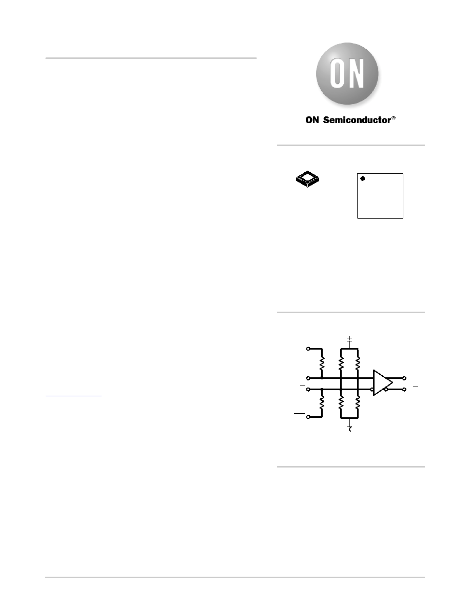
Figure 1. Functional Block Diagram
VTD
D
50 W
VTD
50 W
R1
R2
R1
R2
VEE
VCC
(Note: Microdot may be in either location)
1
相關PDF資料 |
PDF描述 |
|---|---|
| VE-J20-MY | CONVERTER MOD DC/DC 5V 50W |
| DAC8043AFSZ-REEL7 | IC DAC 12BIT MULT SRL INP 8SOIC |
| VI-JWV-MY | CONVERTER MOD DC/DC 5.8V 50W |
| VI-JWT-MY | CONVERTER MOD DC/DC 6.5V 50W |
| LTC1329ACS8-50 | IC D/A CONV 8BIT MICROPWR 8-SOIC |
相關代理商/技術參數 |
參數描述 |
|---|---|
| NB4L339 | 制造商:ONSEMI 制造商全稱:ON Semiconductor 功能描述:3.3V 1:4 Clock Fanout Buffer |
| NB4L339_07 | 制造商:ONSEMI 制造商全稱:ON Semiconductor 功能描述:2.5 V / 3.3 V Differential 2:1 Clock IN to Differential LVPECL Clock Generator / Divider / Fan−Out Buffer |
| NB4L339MNG | 功能描述:時鐘驅動器及分配 2.7V 622MHZ CLK DIST RoHS:否 制造商:Micrel 乘法/除法因子:1:4 輸出類型:Differential 最大輸出頻率:4.2 GHz 電源電壓-最大: 電源電壓-最小:5 V 最大工作溫度:+ 85 C 封裝 / 箱體:SOIC-8 封裝:Reel |
| NB4L339MNGEVB | 功能描述:BOARD EVAL FOR NB4L339MNG RoHS:是 類別:編程器,開發系統 >> 評估演示板和套件 系列:* 標準包裝:1 系列:PCI Express® (PCIe) 主要目的:接口,收發器,PCI Express 嵌入式:- 已用 IC / 零件:DS80PCI800 主要屬性:- 次要屬性:- 已供物品:板 |
| NB4L339MNR2G | 制造商:ONSEMI 制造商全稱:ON Semiconductor 功能描述:2.5 V / 3.3 V Differential 2:1 Clock IN to Differential LVPECL Clock Generator / Divider / Fan−Out Buffer |
發布緊急采購,3分鐘左右您將得到回復。