- 您現(xiàn)在的位置:買賣IC網(wǎng) > PDF目錄2101 > NB4N527SMNR2 (ON Semiconductor)IC DRVR/RCVR/BUFF/XLATOR 16-QFN PDF資料下載
參數(shù)資料
| 型號: | NB4N527SMNR2 |
| 廠商: | ON Semiconductor |
| 文件頁數(shù): | 1/10頁 |
| 文件大小: | 0K |
| 描述: | IC DRVR/RCVR/BUFF/XLATOR 16-QFN |
| 產(chǎn)品變化通告: | Product Discontinuation 20/Aug/2008 |
| 標準包裝: | 3,000 |
| 邏輯類型: | 接收器,驅動器,緩沖器,變換器 |
| 電源電壓: | 3 V ~ 3.6 V |
| 位數(shù): | 2 |
| 工作溫度: | -40°C ~ 85°C |
| 安裝類型: | 表面貼裝 |
| 封裝/外殼: | 16-VFQFN 裸露焊盤 |
| 供應商設備封裝: | 16-QFN(3x3) |
| 包裝: | 帶卷 (TR) |
Semiconductor Components Industries, LLC, 2011
June, 2011 Rev. 5
1
Publication Order Number:
NB4N527S/D
NB4N527S
3.3V, 2.5Gb/s Dual
AnyLevel to LVDS
Receiver/Driver/Buffer/
Translator with Internal
Input Termination
NB4N527S is a clock or data Receiver/Driver/Buffer/Translator
capable of translating AnyLevelTM input signal (LVPECL, CML,
HSTL, LVDS, or LVTTL/LVCMOS) to LVDS. Depending on the
distance, noise immunity of the system design, and transmission line
media, this device will receive, drive or translate data or clock signals
up to 2.5 Gb/s or 1.5 GHz, respectively.
The NB4N527S has a wide input common mode range of
GND + 50 mV to VCC 50 mV combined with two 50 W internal
termination resistors is ideal for translating differential or
singleended data or clock signals to 350 mV typical LVDS output
levels without use of any additional external components (Figure 6).
The device is offered in a small 3 mm x 3 mm QFN16 package.
NB4N527S is targeted for data, wireless and telecom applications as
well as high speed logic interface where jitter and package size are
main requirements. Application notes, models, and support
documentation are available on www.onsemi.com.
Maximum Input Clock Frequency up to 1.5 GHz
Maximum Input Data Rate up to 2.5 Gb/s (Figure 5)
470 ps Maximum Propagation Delay\
1 ps Maximum RMS Jitter
140 ps Maximum Rise/Fall Times
Single Power Supply; VCC = 3.3 V $10%
Temperature Compensated TIA/EIA644 Compliant LVDS Outputs
Internal 50 W Termination Resistor per Input Pin
GND + 50 mV to VCC 50 mV VCMR Range
These are PbFree Devices
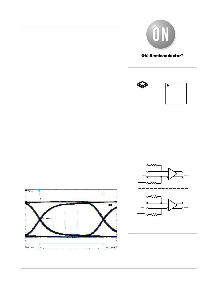
TIME (58 ps/div)
Figure 2. Typical Output Waveform at 2.488 Gb/s with
PRBS 2231 (VINPP = 400 mV; Input Signal DDJ = 14 ps)
VOL
TAGE
(130
mV/div)
Device DDJ = 10 ps
A
= Assembly Location
L
= Wafer Lot
Y
= Year
W
= Work Week
G
= PbFree Package
*For additional marking information, refer to
Application Note AND8002/D.
MARKING
DIAGRAM*
QFN16
MN SUFFIX
CASE 485G
http://onsemi.com
See detailed ordering and shipping information in the package
dimensions section on page 9 of this data sheet.
ORDERING INFORMATION
16
NB4N
527S
ALYW G
G
1
Q0
Figure 1. Functional Block Diagram
VTD0
D0
Q1
D0
50 W*
D1
VTD0
50 W*
VTD1
1
*RTIN
(Note: Microdot may be in either location)
相關PDF資料 |
PDF描述 |
|---|---|
| NB4N855SMR4G | IC DRVR/RCVR/BUFF/XLATOR MICRO10 |
| NB6HQ14MMNG | IC CLK BUFF MUX 1:4 5GHZ 16-QFN |
| NB6L11DTR2 | IC CLK BUFFER TRANSLA 1:2 8TSSOP |
| NB6L11SMNR2G | IC CLK BUFFER TRANSLA 1:2 16-QFN |
| NB6L14MNG | IC CLOCK BUFFER 1:4 3GHZ 16-QFN |
相關代理商/技術參數(shù) |
參數(shù)描述 |
|---|---|
| NB4N527SMNR2G | 功能描述:時鐘驅動器及分配 3.3V 2.5Gb/s Dual Driver/RCVR/Buffer RoHS:否 制造商:Micrel 乘法/除法因子:1:4 輸出類型:Differential 最大輸出頻率:4.2 GHz 電源電壓-最大: 電源電壓-最小:5 V 最大工作溫度:+ 85 C 封裝 / 箱體:SOIC-8 封裝:Reel |
| NB4N7132 | 制造商:ONSEMI 制造商全稱:ON Semiconductor 功能描述:Link Replicator for Fibre Channel, Gigabit Ethernet, HDTV and SATA |
| NB4N7132DTG | 功能描述:通信集成電路 - 若干 2.5 GBPS SER LNK REP RoHS:否 制造商:Maxim Integrated 類型:Transport Devices 封裝 / 箱體:TECSBGA-256 數(shù)據(jù)速率:100 Mbps 電源電壓-最大:1.89 V, 3.465 V 電源電壓-最小:1.71 V, 3.135 V 電源電流:50 mA, 225 mA 最大工作溫度:+ 85 C 最小工作溫度:- 40 C 封裝:Tube |
| NB4N7132DTR2G | 功能描述:通信集成電路 - 若干 2.5 GBPS SER LNK REP RoHS:否 制造商:Maxim Integrated 類型:Transport Devices 封裝 / 箱體:TECSBGA-256 數(shù)據(jù)速率:100 Mbps 電源電壓-最大:1.89 V, 3.465 V 電源電壓-最小:1.71 V, 3.135 V 電源電流:50 mA, 225 mA 最大工作溫度:+ 85 C 最小工作溫度:- 40 C 封裝:Tube |
| NB4N840M | 制造商:ONSEMI 制造商全稱:ON Semiconductor 功能描述:3.3V 3.2Gb/s Dual Differential Clock/Data 2 x 2 Crosspoint Switch with CML Output and Internal Termination |
發(fā)布緊急采購,3分鐘左右您將得到回復。