參數資料
| 型號: | NB4N840MMNG |
| 廠商: | ON Semiconductor |
| 文件頁數: | 1/10頁 |
| 文件大小: | 0K |
| 描述: | IC CROSSPOINT SWITCH DUAL 32QFN |
| 標準包裝: | 74 |
| 功能: | 交叉點開關 |
| 電路: | 2 x 2:2 |
| 電壓電源: | 單電源 |
| 電壓 - 電源,單路/雙路(±): | 3 V ~ 3.6 V |
| 電流 - 電源: | 130mA |
| 工作溫度: | -40°C ~ 85°C |
| 安裝類型: | 表面貼裝 |
| 封裝/外殼: | 32-VFQFN 裸露焊盤 |
| 供應商設備封裝: | 32-QFN(5x5) |
| 包裝: | 托盤 |
Semiconductor Components Industries, LLC, 2011
June, 2011 Rev. 4
1
Publication Order Number:
NB4N840M/D
NB4N840M
3.3V 3.2Gb/s Dual
Differential Clock/Data 2 x 2
Crosspoint Switch with
CML Output and Internal
Termination
Description
The NB4N840M is a highbandwidth fully differential dual
2 x 2 crosspoint switch with CML inputs/outputs that is suitable for
applications such as SDH/SONET, DWDM, Gigabit Ethernet and
high speed switching. Fully differential design techniques are used to
minimize jitter accumulation, crosstalk, and signal skew, which make
this device ideal for loopthrough and protection channel switching
applications.
Internally terminated differential CML inputs accept ACcoupled
LVPECL (Positive ECL) or direct coupled CML signals. By providing
internal 50
W input and output termination resistor, the need for
external components is eliminated and interface reflections are
minimized. Differential 16 mA CML outputs provide matching
internal 50
W terminations, and 400 mV output swings when
externally terminated, 50
W to VCC.
Singleended LVCMOS/LVTTL SEL inputs control the routing of
the signals through the crosspoint switch which makes this device
configurable as 1:2 fanout, repeater or 2 x 2 crosspoint switch. The
device is housed in a low profile 5 x 5 mm 32pin QFN package.
Features
Plugin compatible to the MAX3840 and SY55859L
Maximum Input Clock Frequency 2.7 GHz
Maximum Input Data Frequency 3.2 Gb/s
225 ps Typical Propagation Delay
80 ps Typical Rise and Fall Times
7 ps Channel to Channel Skew
430 mW Power Consumption
< 0.5 ps RMS Jitter
7 ps PeaktoPeak Data Dependent Jitter
Power Saving Feature with Disabled Outputs
Operating Range: VCC = 3.0 V to 3.6 V with VEE = 0 V
CML Output Level (400 mV PeaktoPeak Output), Differential
Output
These are PbFree Devices
QFN32
MN SUFFIX
CASE 488AM
See detailed ordering and shipping information on page 9 of
this data sheet.
ORDERING INFORMATION
MARKING
DIAGRAM
http://onsemi.com
32
1
NB4N
840M
ALYWG
1
A
= Assembly Location
WL
= Wafer Lot
YY
= Year
WW
= Work Week
G
= PbFree Package
CML
0
1
0
1
0
1
0
1
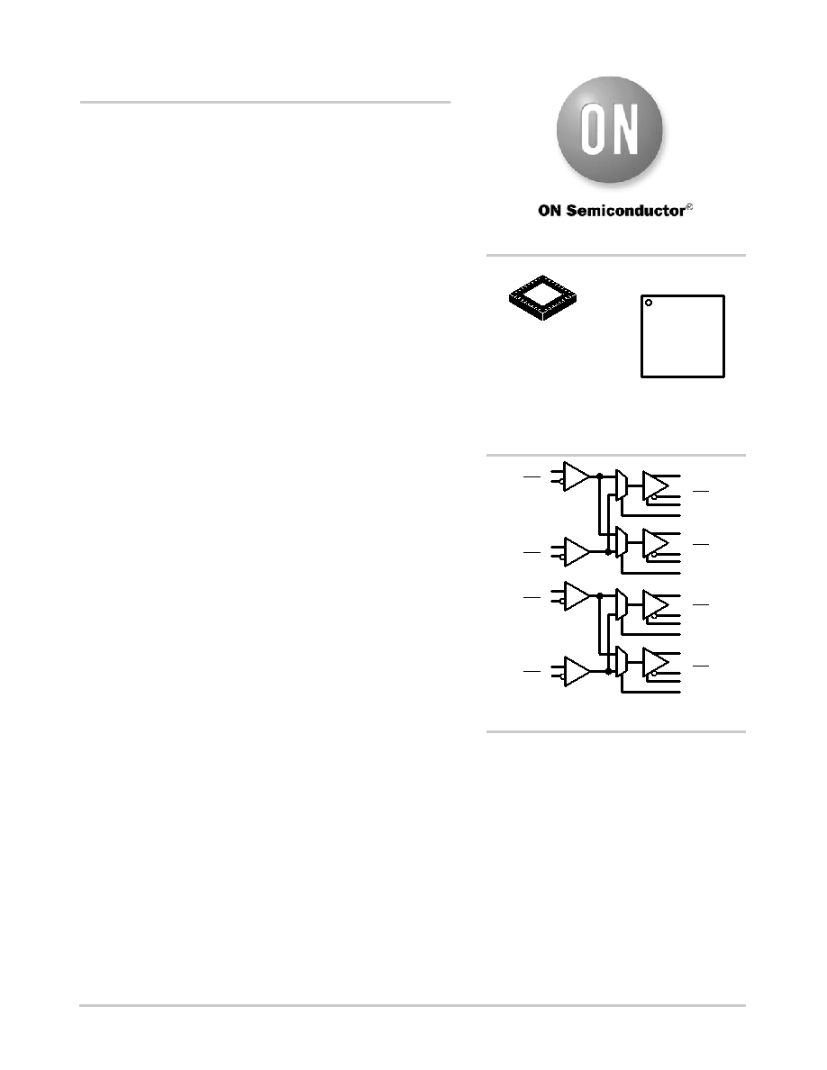
Figure 1. Functional Block Diagram
QA0
ENA0
SELA0
QA1
ENA1
SELA1
QB0
ENB0
SELB0
QB1
ENB1
SELB1
DA0
DA1
DB0
DB1
相關PDF資料 |
PDF描述 |
|---|---|
| NB6L72MMNG | IC CROSSPOINT SWITCH 2X2 16QFN |
| NB6L72MNR2G | IC CROSSPOINT SWITCH 2X2 16QFN |
| NB7L72MMNHTBG | IC CROSSPOINT SW 2X2 DIFF 16-QFN |
| NB7V72MMNG | IC CROSSPOINT SWITCH 2X2 16QFN |
| NBSG16BAHTBG | IC RCVR/DVR RSECL SIGE 16FCBGA |
相關代理商/技術參數 |
參數描述 |
|---|---|
| NB4N840MMNR4G | 功能描述:模擬和數字交叉點 IC ANA 2X2 CROSSPT SWCH CML RoHS:否 制造商:Micrel 配置:2 x 2 封裝 / 箱體:MLF-16 數據速率:10.7 Gbps 輸入電平:CML, LVDS, LVPECL 輸出電平:CML 電源電壓-最大:3.6 V 電源電壓-最小:2.375 V 最大工作溫度:+ 85 C 最小工作溫度:- 40 C 產品:Digital Crosspoint 封裝:Tube |
| NB4N840MMNTWG | 制造商:ON Semiconductor 功能描述:DUAL DIFF 2X2 SWITCH - Tape and Reel |
| NB4N855S | 制造商:ONSEMI 制造商全稱:ON Semiconductor 功能描述:3.3 V, 1.5 Gb/s Dual AnyLevelTM to LVDS Receiver/Driver/Buffer/ Translator |
| NB4N855S_06 | 制造商:ONSEMI 制造商全稱:ON Semiconductor 功能描述:3.3 V, 1.5 Gb/s Dual AnyLevel TM to LVDS Receiver/Driver/Buffer/ Translator |
| NB4N855SMEVB | 功能描述:CUSTOMER EVALUATION BRD RoHS:是 類別:編程器,開發系統 >> 評估演示板和套件 系列:* 標準包裝:1 系列:PCI Express® (PCIe) 主要目的:接口,收發器,PCI Express 嵌入式:- 已用 IC / 零件:DS80PCI800 主要屬性:- 次要屬性:- 已供物品:板 |
發布緊急采購,3分鐘左右您將得到回復。