參數資料
| 型號: | NB7VPQ16MMNG |
| 廠商: | ON Semiconductor |
| 文件頁數: | 1/16頁 |
| 文件大小: | 0K |
| 描述: | IC CML PRE-EMPH DRIVER 16QFN |
| 標準包裝: | 123 |
| 邏輯類型: | CML 驅動器,帶可選均衡器接收器 |
| 電源電壓: | 1.71 V ~ 2.625 V |
| 工作溫度: | -40°C ~ 85°C |
| 安裝類型: | 表面貼裝 |
| 封裝/外殼: | 16-VFQFN 裸露焊盤 |
| 供應商設備封裝: | 16-QFN(3x3) |
| 包裝: | 管件 |
Semiconductor Components Industries, LLC, 2009
July, 2009 Rev. 0
1
Publication Order Number:
NB7VPQ16M/D
NB7VPQ16M
1.8V/2.5V CML 12.5 Gbps
Programmable Pre-Emphasis
Copper/Cable Driver with
Selectable Equalizer Receiver
MultiLevel Inputs w/ Internal Termination
Description
The NB7VPQ16M is a high performance single channel
programmable PreEmphasis CML Driver with a selectable Equalizer
Receiver that operates up to 14 Gbps typical with a 1.8 V or 2.5 V
power supply. When placed in series with a Data/Clock path, the
NB7VPQ16M inputs will compensate the degraded signal transmitted
across a FR4 PCB backplane or cable interconnect. Therefore, the
serial data rate is increased by reducing InterSymbol Interference
(ISI) caused by losses in copper interconnect or long cables.
The PreEmphasis buffer is controlled using a serial bus via the
Serial Data In (SDIN) and Serial Clock In (SCLKIN) control inputs
and contains circuitry which provides sixteen programmable
PreEmphasis settings to select the optimal output compensation
level.
These selectable output levels will handle various backplane lengths
and cable lines. The first four SDIN bits (D3:D0) will digitally select
0 dB through 12 dB typical of deemphasis (see Table 1).
For cascaded applications, the shifted SDIN and SCLKIN signals
are presented at the SDOUT and SCLKOUT pins.
The 5thbit (LSB) of the serial data bits allows for enabling the
equalization function of the receiver.
The differential Data / Clock inputs incorporate a pair of internal
50
W termination resistors, in a 100 W centertapped configuration,
via the VT pin and will accept LVPECL, CML or LVDS logic levels.
This feature provides transmission line termination onchip, at the
receiver end, eliminating external components.
The NB7VPQ16M is a member of the GigaComm
Family of high
performance Data/Clock products with PreEmphasis/Equalization
(PEEQ).
Features
Maximum Input Data Rate > 12.5 Gbps
Maximum Input Clock Frequency > 8 GHz
Drives Up To 18inches of FR4
(16) Programmable Output Deemphasis Levels; 0 dB
through 12 dB
200 ps Typical Propagation Delay
Differential CML Outputs, 400 mV PeaktoPeak,
Typical (PE = 0 dB)
Operating Range: VCC = 1.71 V to 2.625 V, GND = 0 V
Internal Output Termination Resistors, 50 W
QFN16 Package, 3 mm x 3 mm
40°C to +85°C Ambient Operating Temperature
These are PbFree Devices
A
= Assembly Location
L
= Wafer Lot
Y
= Year
W
= Work Week
G
= PbFree Package
*For additional marking information, refer to
Application Note AND8002/D.
MARKING
DIAGRAM*
QFN16
MN SUFFIX
CASE 485G
http://onsemi.com
See detailed ordering and shipping information in the package
dimensions section on page 15 of this data sheet.
ORDERING INFORMATION
16
NB7V
PQ16M
ALYWG
G
1
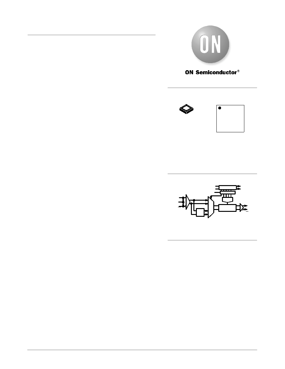
Figure 1. Simplified Logic Diagram
(Note: Microdot may be in either location)
SDI
DAC
PE
EQ
SDOUT
SCLKOUT
Q
SDIN
SCLKIN
SLOAD
Q
IN
VT
1
相關PDF資料 |
PDF描述 |
|---|---|
| NB7VQ1006MMNG | IC EQUALIZER RECEIVER 24-QFN |
| NB7VQ14MMNG | IC CLOCK BUFFER MUX 1:4 16-QFN |
| NB7VQ58MMNHTBG | IC CLOCK/DATA MUX 2:1 7GHZ 16QFN |
| NBSG11BAHTBG | IC CLK BUFFER 1:2 12GHZ 16-FCBGA |
| NBSG14BAHTBG | IC CLOCK/DATA BUFFER 1:4 16FCBGA |
相關代理商/技術參數 |
參數描述 |
|---|---|
| NB7VPQ16MMNGM | 制造商:Rochester Electronics LLC 功能描述: 制造商:ON Semiconductor 功能描述: |
| NB7VPQ16MMNHTBG | 功能描述:時鐘驅動器及分配 EQU/PREEMP SNGLE CHN RoHS:否 制造商:Micrel 乘法/除法因子:1:4 輸出類型:Differential 最大輸出頻率:4.2 GHz 電源電壓-最大: 電源電壓-最小:5 V 最大工作溫度:+ 85 C 封裝 / 箱體:SOIC-8 封裝:Reel |
| NB7VPQ16MMNTXG | 功能描述:緩沖器和線路驅動器 EQU/PREEMP SNGL CHAN RoHS:否 制造商:Micrel 輸入線路數量:1 輸出線路數量:2 極性:Non-Inverting 電源電壓-最大:+/- 5.5 V 電源電壓-最小:+/- 2.37 V 最大工作溫度:+ 85 C 安裝風格:SMD/SMT 封裝 / 箱體:MSOP-8 封裝:Reel |
| NB7VQ1006M | 制造商:ONSEMI 制造商全稱:ON Semiconductor 功能描述:1.8V / 2.5V 10Gbps Equalizer Receiver with 1:6 Differential CML Outputs |
| NB7VQ1006MMNG | 功能描述:IC EQUALIZER RECEIVER 24-QFN RoHS:是 類別:集成電路 (IC) >> 邏輯 - 專用邏輯 系列:- 產品變化通告:Product Discontinuation 25/Apr/2012 標準包裝:1,500 系列:74SSTV 邏輯類型:DDR 的寄存緩沖器 電源電壓:2.3 V ~ 2.7 V 位數:14 工作溫度:0°C ~ 70°C 安裝類型:表面貼裝 封裝/外殼:48-TFSOP(0.240",6.10mm 寬) 供應商設備封裝:48-TSSOP 包裝:帶卷 (TR) |
發布緊急采購,3分鐘左右您將得到回復。