- 您現在的位置:買賣IC網 > PDF目錄361076 > NBSG53ABA (ON SEMICONDUCTOR) 2.5V/3.3V SiGe Selectable Differential Clock and Data D Flip-Flop/Clock Divider with Reset and OLS PDF資料下載
參數資料
| 型號: | NBSG53ABA |
| 廠商: | ON SEMICONDUCTOR |
| 元件分類: | 時鐘及定時 |
| 英文描述: | 2.5V/3.3V SiGe Selectable Differential Clock and Data D Flip-Flop/Clock Divider with Reset and OLS |
| 中文描述: | 53 SERIES, LOW SKEW CLOCK DRIVER, 1 TRUE OUTPUT(S), 0 INVERTED OUTPUT(S), PBGA16 |
| 封裝: | 4 X 4 MM, PLASTIC, FCBGA-16 |
| 文件頁數: | 2/18頁 |
| 文件大小: | 133K |
| 代理商: | NBSG53ABA |
NBSG53A
http://onsemi.com
2
VTD
CLK
CLK
VTCLK
V
CC
R
VTCLK
D
D
VTD
V
CC
V
EE
SEL
OLS
Q
Q
A
B
C
D
1
2
3
4
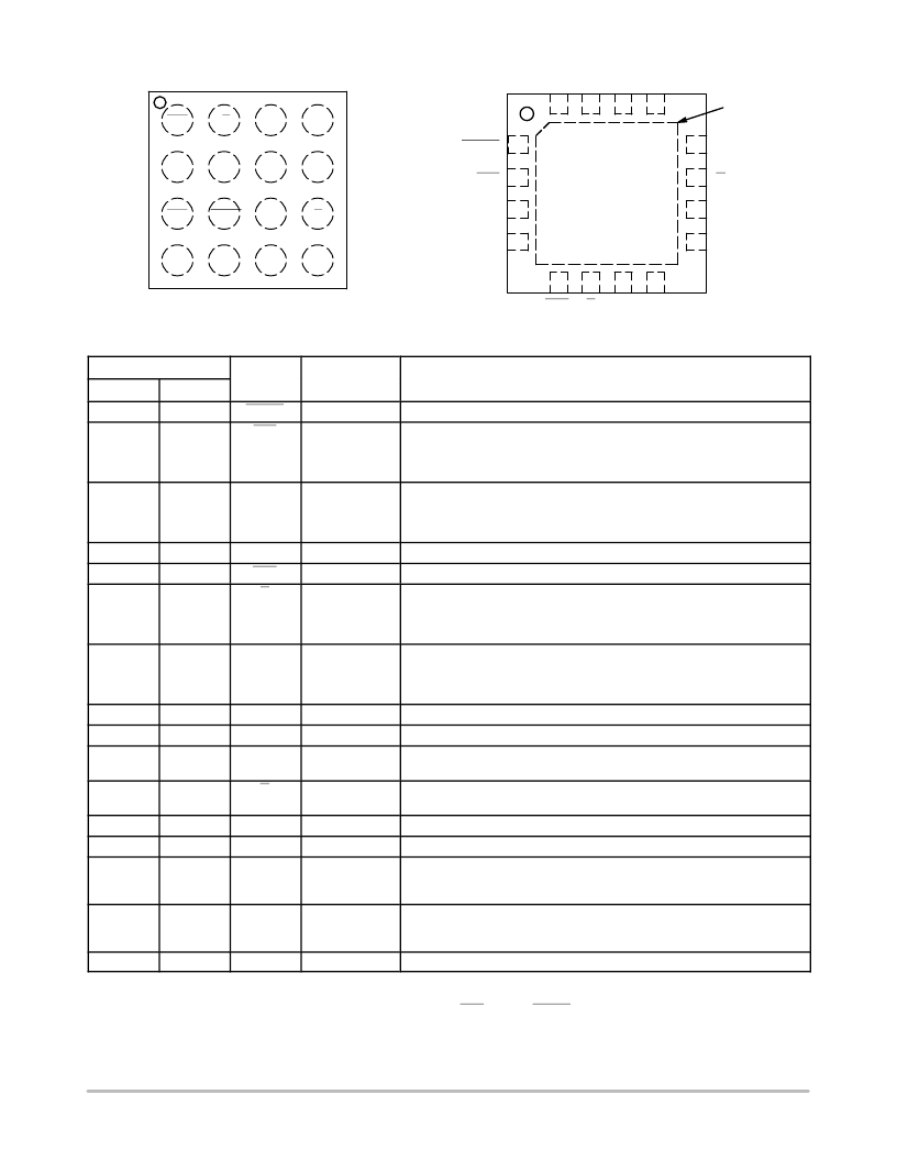
Figure 1. BGA16 Pinout
(Top View)
VTD
D
D
VTD
V
CC
R
SEL OLS
V
EE
Q
Q
V
CC
VTCLK
CLK
CLK
VTCLK
5
6
7
8
16
15
14
13
12
11
10
9
1
2
3
4
NBSG53A
Exposed Pad
(EP)
Figure 2. QFN16 Pinout
(Top View)
Table 1. Pin Description
Pin
BGA
QFN
Name
VTCLK
I/O
Description
C2
1
Internal 50 Termination Pin. See Table 4.
C1
2
CLK
ECL, CML,
LVCMOS,
LVDS, LVTTL
Input
Inverted Differential Input.
B1
3
CLK
ECL, CML,
LVCMOS,
LVDS, LVTTL
Input
Noninverted Differential Input.
B2
4
VTCLK
Internal 50 Termination Pin. See Table 4.
A1
5
VTD
Internal 50 termination pin. See Table 4.
A2
6
D
ECL, CML,
LVCMOS,
LVDS, LVTTL
Input
Inverted Differential Input.
A3
7
D
ECL, CML,
LVCMOS,
LVDS, LVTTL
Input
Noninverted Differential Input.
A4
8
VTD
Internal 50 Termination Pin. See Table 4.
D1,B3
9,16
V
CC
Q
Positive Supply Voltage
B4
10
RSECL Output
Inverted Differential Output. Typically Terminated with 50 Resistor to
V
TT
= V
CC
2 V.
C4
11
Q
RSECL Output
Noninverted Differential Output. Typically Terminated with 50 Resistor to
V
TT
= V
CC
2 V.
C3
12
V
EE
OLS*
Negative Supply Voltage
D4
13
Input
Input Pin for the Output Level Select (OLS). See Table 2.
D3
14
SEL
LVECL,
LVCMOS,
LVTTL Input
Select Logic Input. Internal 75 k to V
EE
.
D2
15
R
LVECL,
LVCMOS,
LVTTL Input
Reset D FlipFlop. Internal 75 k to V
EE
.
N/A
EP
Exposed Pad. (Note 1)
1. All V
and V
pins must be externally connected to Power Supply to guarantee proper operation. The thermally exposed pad (EP) on
package bottom (see case drawing) must be attached to a heatsinking conduit.
2. In the differential configuration when the input termination pins (VTD, VTD, VTCLK, VTCLK) are connected to a common termination volt-
age, and if no signal is applied then the device will be susceptible to selfoscillation.
3. When an output level of 400 mV is desired and V
CC
V
EE
> 3.0 V, 2K resistor should be connected from OLS pin to V
EE
.
相關PDF資料 |
PDF描述 |
|---|---|
| NBSG53ABAR2 | 2.5V/3.3V SiGe Selectable Differential Clock and Data D Flip-Flop/Clock Divider with Reset and OLS |
| NBSG53AMN | 2.5V/3.3V SiGe Selectable Differential Clock and Data D Flip-Flop/Clock Divider with Reset and OLS |
| NBXDBA014 | 3.3 V, 62.5 MHz / 125 MHz LVPECL Clock Oscillator |
| NBXDBA014LN1TAG | 3.3 V, 62.5 MHz / 125 MHz LVPECL Clock Oscillator |
| NC12S0A0H06NNFA | Delphi NC06 Series Non-Isolated Point of Load DC/DC Power Modules: 12Vin, 0.9V~5.0Vout, 6A |
相關代理商/技術參數 |
參數描述 |
|---|---|
| NBSG53ABAEVB | 功能描述:時鐘和定時器開發工具 BBG NBSG53ABA EVAL BOARD RoHS:否 制造商:Texas Instruments 產品:Evaluation Modules 類型:Clock Conditioners 工具用于評估:LMK04100B 頻率:122.8 MHz 工作電源電壓:3.3 V |
| NBSG53ABAHTBG | 功能描述:時鐘驅動器及分配 2.5/3.3V SEL DIFF CLK RoHS:否 制造商:Micrel 乘法/除法因子:1:4 輸出類型:Differential 最大輸出頻率:4.2 GHz 電源電壓-最大: 電源電壓-最小:5 V 最大工作溫度:+ 85 C 封裝 / 箱體:SOIC-8 封裝:Reel |
| NBSG53ABAR2 | 功能描述:觸發器 2.5V/3.3V SiGe Diff RoHS:否 制造商:Texas Instruments 電路數量:2 邏輯系列:SN74 邏輯類型:D-Type Flip-Flop 極性:Inverting, Non-Inverting 輸入類型:CMOS 輸出類型: 傳播延遲時間:4.4 ns 高電平輸出電流:- 16 mA 低電平輸出電流:16 mA 電源電壓-最大:5.5 V 最大工作溫度:+ 85 C 安裝風格:SMD/SMT 封裝 / 箱體:X2SON-8 封裝:Reel |
| NBSG53AMA1TBG | 制造商:ON Semiconductor 功能描述:SIGE DIF CLK DATA D F-F - Tape and Reel |
| NBSG53AMAG | 功能描述:IC FLIP FLOP/CLK DIVIDER 16FCLGA RoHS:是 類別:集成電路 (IC) >> 邏輯 - 觸發器 系列:- 產品變化通告:Product Discontinuation 27/Jan/2012 標準包裝:2,000 系列:74LCX 功能:標準 類型:D 型總線 輸出類型:三態非反相 元件數:1 每個元件的位元數:8 頻率 - 時鐘:150MHz 延遲時間 - 傳輸:1.5ns 觸發器類型:正邊沿 輸出電流高,低:24mA,24mA 電源電壓:2 V ~ 3.6 V 工作溫度:-40°C ~ 85°C 安裝類型:表面貼裝 封裝/外殼:20-SOIC(0.209",5.30mm 寬) 包裝:帶卷 (TR) 其它名稱:MC74LCX574MELG-NDMC74LCX574MELGOSTR |
發布緊急采購,3分鐘左右您將得到回復。