- 您現在的位置:買賣IC網 > PDF目錄361076 > NBSG53ABAEVB (ON SEMICONDUCTOR) LJT 61C 61#20 PIN PLUG PDF資料下載
參數資料
| 型號: | NBSG53ABAEVB |
| 廠商: | ON SEMICONDUCTOR |
| 英文描述: | LJT 61C 61#20 PIN PLUG |
| 中文描述: | 2.5V/3.3V的硅鍺可選差分時鐘和數據d Flip-Flop/Clock除法的復位和生命線行動 |
| 文件頁數: | 1/18頁 |
| 文件大小: | 133K |
| 代理商: | NBSG53ABAEVB |
Semiconductor Components Industries, LLC, 2004
March, 2004 Rev. 5
1
Publication Order Number:
NBSG53A/D
NBSG53A
2.5V/3.3VSiGe Selectable
Differential Clock and Data
D FlipFlop/Clock Divider
with Reset and OLS*
The NBSG53A is a multifunction differential D flipflop (DFF) or
fixed divide by two (DIV/2) clock generator. This is a part of the
GigaComm
family of high performance Silicon Germanium
products. A strappable control pin is provided to select between the
two functions. The device is housed in a low profile 4x4 mm 16pin
FlipChip BGA (FCBGA) or a 3x3 mm 16 pin QFN package.
The NBSG53A is a device with data, clock, OLS, reset, and select
inputs. Differential inputs incorporate internal 50
resistors and accept NECL (Negative ECL), PECL (Positive ECL),
LVCMOS/LVTTL, CML, or LVDS. The OLS input is used to
program the peaktopeak output amplitude between 0 and 800 mV
in five discrete steps. The RESET and SELECT inputs are
singleended and can be driven with either LVECL or
LVCMOS/LVTTL input levels.
Data is transferred to the outputs on the positive edge of the clock.
The differential clock inputs of the NBSG53A allow the device to also
be used as a negative edge triggered device.
Maximum Input Clock Frequency (DFF) > 8 GHz Typical
(See Figures 4, 6, 8, 10, and 11)
Maximum Input Clock Frequency (DIV/2) > 10 GHz Typical
(See Figures 5, 7, 9, 10, and 11)
210 ps Typical Propagation Delay (OLS = FLOAT)
45 ps Typical Rise and Fall Times (OLS = FLOAT)
DIV/2 Mode (Active with Select Low)
DFF Mode (Active with Select High)
Selectable Swing PECL Output with Operating Range: V
CC
= 2.375 V
to 3.465 V with V
EE
= 0 V
Selectable Swing NECL Output with NECL Inputs with
Operating Range: V
CC
= 0 V with V
EE
= 2.375 V to 3.465 V
Selectable Output Level (0 V, 200 mV, 400 mV, 600 mV, or 800 mV
PeaktoPeak Output)
50 Internal Input Termination Resistors on all Differential Inputs
*Output Level Select
termination
**For further details, refer to Application
Note AND8002/D
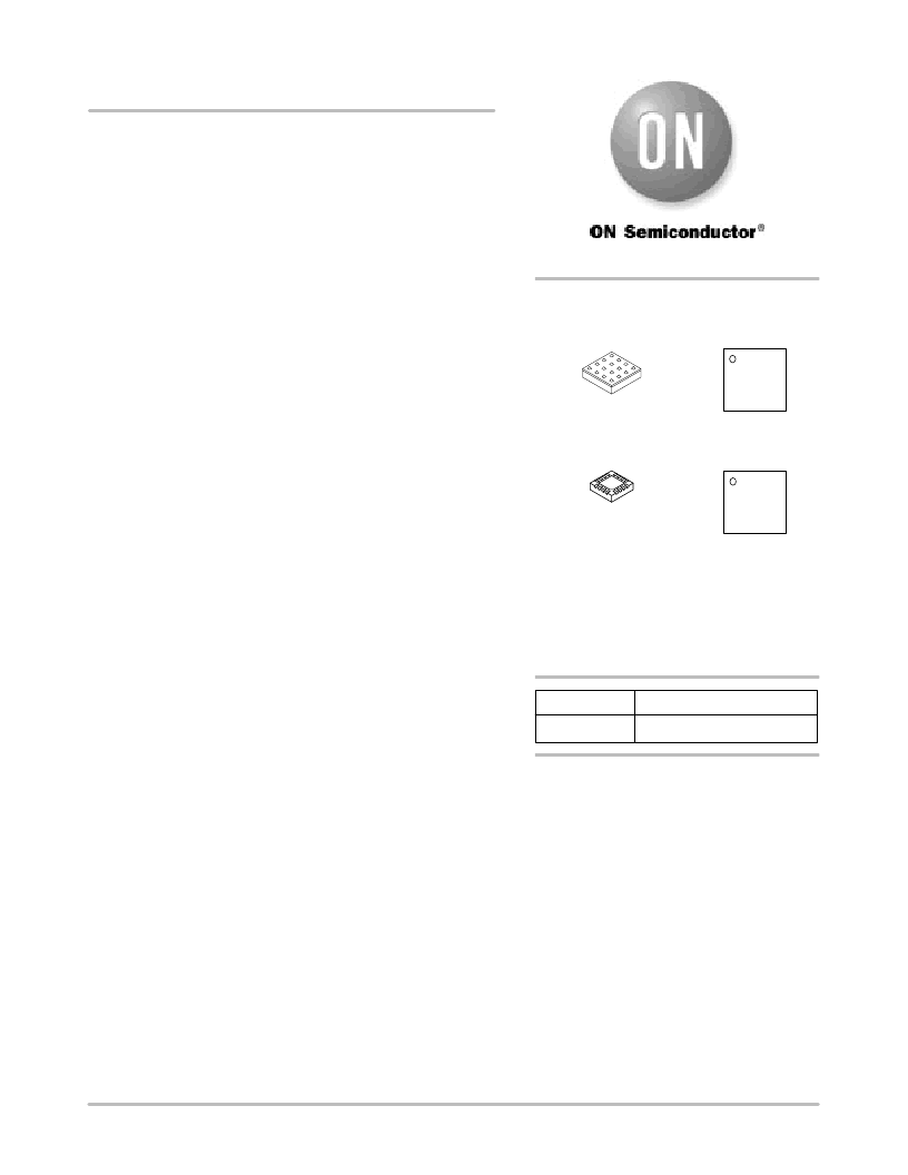
FCBGA16
BA SUFFIX
CASE 489
MARKING
DIAGRAM**
SG
53A
LYW
Board
Description
NBSG53ABAEVB
NBSG53ABA Evaluation Board
http://onsemi.com
A = Assembly Location
L = Wafer Lot
Y = Year
W= Work Week
SG53A
ALYW
QFN16
MN SUFFIX
CASE 485G
See detailed ordering and shipping information in the package
dimensions section on page 16 of this data sheet.
ORDERING INFORMATION
相關PDF資料 |
PDF描述 |
|---|---|
| NBSG53ABA | 2.5V/3.3V SiGe Selectable Differential Clock and Data D Flip-Flop/Clock Divider with Reset and OLS |
| NBSG53ABAR2 | 2.5V/3.3V SiGe Selectable Differential Clock and Data D Flip-Flop/Clock Divider with Reset and OLS |
| NBSG53AMN | 2.5V/3.3V SiGe Selectable Differential Clock and Data D Flip-Flop/Clock Divider with Reset and OLS |
| NBXDBA014 | 3.3 V, 62.5 MHz / 125 MHz LVPECL Clock Oscillator |
| NBXDBA014LN1TAG | 3.3 V, 62.5 MHz / 125 MHz LVPECL Clock Oscillator |
相關代理商/技術參數 |
參數描述 |
|---|---|
| NBSG53ABAHTBG | 功能描述:時鐘驅動器及分配 2.5/3.3V SEL DIFF CLK RoHS:否 制造商:Micrel 乘法/除法因子:1:4 輸出類型:Differential 最大輸出頻率:4.2 GHz 電源電壓-最大: 電源電壓-最小:5 V 最大工作溫度:+ 85 C 封裝 / 箱體:SOIC-8 封裝:Reel |
| NBSG53ABAR2 | 功能描述:觸發器 2.5V/3.3V SiGe Diff RoHS:否 制造商:Texas Instruments 電路數量:2 邏輯系列:SN74 邏輯類型:D-Type Flip-Flop 極性:Inverting, Non-Inverting 輸入類型:CMOS 輸出類型: 傳播延遲時間:4.4 ns 高電平輸出電流:- 16 mA 低電平輸出電流:16 mA 電源電壓-最大:5.5 V 最大工作溫度:+ 85 C 安裝風格:SMD/SMT 封裝 / 箱體:X2SON-8 封裝:Reel |
| NBSG53AMA1TBG | 制造商:ON Semiconductor 功能描述:SIGE DIF CLK DATA D F-F - Tape and Reel |
| NBSG53AMAG | 功能描述:IC FLIP FLOP/CLK DIVIDER 16FCLGA RoHS:是 類別:集成電路 (IC) >> 邏輯 - 觸發器 系列:- 產品變化通告:Product Discontinuation 27/Jan/2012 標準包裝:2,000 系列:74LCX 功能:標準 類型:D 型總線 輸出類型:三態非反相 元件數:1 每個元件的位元數:8 頻率 - 時鐘:150MHz 延遲時間 - 傳輸:1.5ns 觸發器類型:正邊沿 輸出電流高,低:24mA,24mA 電源電壓:2 V ~ 3.6 V 工作溫度:-40°C ~ 85°C 安裝類型:表面貼裝 封裝/外殼:20-SOIC(0.209",5.30mm 寬) 包裝:帶卷 (TR) 其它名稱:MC74LCX574MELG-NDMC74LCX574MELGOSTR |
| NBSG53AMN | 功能描述:觸發器 2.5V/3.3V SiGe Diff RoHS:否 制造商:Texas Instruments 電路數量:2 邏輯系列:SN74 邏輯類型:D-Type Flip-Flop 極性:Inverting, Non-Inverting 輸入類型:CMOS 輸出類型: 傳播延遲時間:4.4 ns 高電平輸出電流:- 16 mA 低電平輸出電流:16 mA 電源電壓-最大:5.5 V 最大工作溫度:+ 85 C 安裝風格:SMD/SMT 封裝 / 箱體:X2SON-8 封裝:Reel |
發布緊急采購,3分鐘左右您將得到回復。