- 您現(xiàn)在的位置:買賣IC網(wǎng) > PDF目錄361089 > NCN6010D (ON SEMICONDUCTOR) SIM Card Supply and Level Shifter PDF資料下載
參數(shù)資料
| 型號(hào): | NCN6010D |
| 廠商: | ON SEMICONDUCTOR |
| 英文描述: | SIM Card Supply and Level Shifter |
| 中文描述: | SIM卡供應(yīng)和電平轉(zhuǎn)換器 |
| 文件頁數(shù): | 3/16頁 |
| 文件大小: | 173K |
| 代理商: | NCN6010D |
NCN6010
http://onsemi.com
3
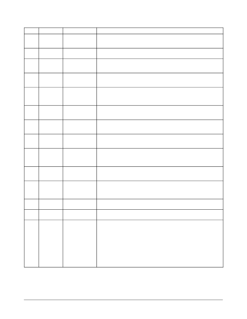
PIN DESCRIPTIONS
Pin
Name
Type
Description
1
V
DD
POWER
This pin is connected to the system controller power supply suitable to operate from
a 3.6 V typical battery. A low ESR ceramic capacitor (4.7 F typical) shall be used to
bypass the power supply voltage.
2
STOP
INPUT
A Low level on this pin resets the SIM interface, switching off the SIM_VCC,
according to the ISO7816–3 Power Down procedure (See Table 1 and Figure 3).
3
MOD_V
CC
INPUT
The signal present on this pin programs the SIM_VCC value (See Table 1):
MOD_VCC = L
→
SIM_VCC = 5.0 V
MOD_VCC = H
→
SIM_VCC = 3.0 V
4
PWR_ON
INPUT
The signal present on this pin controls the SIM_VCC state (See Table 1):
PWR_ON = L
→
SIM_VCC = Open, no supply connected to the SIM card.
PWR_ON = H
→
SIM_VCC = Active, the card is powered.
5
I/O
INPUT
This pin is connected to an external microcontroller or GSM management unit. A
bi–directional level translator adapts the serial I/O signal between the smart card and
the external controller. A built–in constant 20 k
(typical) resistor provides a high
impedance state when not activated.
6
CLOCK
INPUT
The clock signal, coming from the external controller, must have a Duty Cycle within
the Min/Max values defined by the specification (typically 50%). The built–in level
shifter translates the input signal to the external SIM card CLK input.
7
RESET
INPUT
The RESET signal present at this pin is connected to the SIM card. The internal level
shifter translates the level according to the voltages present at pin 1 and the
SIM_VCC programmed value.
8
SIM_RST
OUTPUT
This pin is connected to the RESET pin of the card connector. A level translator
adapts the external RESET signal to the SIM card. A built–in active pull down
connects this pin to ground when the device is in a nonoperating mode.
9
SIM_CLK
OUTPUT
This pin is connected to the CLK pin of the card connector. The CLOCK signal
comes from the external clock generator, the internal level shifter being used to
adapt the voltage defined for the SIM_VCC. A built–in active pull down connects this
pin to ground when the device is in a nonoperating mode.
10
GND
GROUND
This pin is the GROUND reference for the integrated circuit and associated signals.
Cares must be observed to avoid voltage spikes when the device operates in a
normal operation.
11
SIM_I/O
This pin handles the connection to the serial I/O of the card connector. A
bi–directional level translator adapts the serial I/O signal between the card and the
microcontroller. A 20 k
(typical) pull up resistor provides a High impedance state for
the SIM card I/O link.
12
Cta
POWER
This pin is connected to the external capacitor used by the internal Charge Pump
converter. Using Low ESR ceramic type is recommended (X5R or X7R).
13
Ctb
POWER
This pin is connected to the external capacitor used by the internal Charge Pump
converter. Using Low ESR ceramic type is recommended (X5R or X7R).
14
SIM_VCC
POWER
This pin is connected to the SIM card power supply pin. An internal Charge Pump
converter is programmable by the external MPU to supply either 3.0 V or 5.0 V
output voltage. An external 1.0
μ
F minimum ceramic capacitor (ESR
X5R or X7R recommended) must be connected across SIM_VCC and GND.
100 m ,
During a normal operation, the SIM_VCC voltage can be set to 3.0 V followed by a
5.0 V value, or can start directly to any of these two values. When the voltage is
adjusted downward (from 5.0 V to 3.0 V) cares must be observed as reverse peak
current can flow from the external capacitors to the battery during a short amount of
time (in the 1.0
μ
s range). When such a voltage adjustment is necessary, it is
recommended to force SIM_VCC to zero, wait 350
μ
s minimum, then reprogram the
chip to get SIM_VCC = 3.0 V.
相關(guān)PDF資料 |
PDF描述 |
|---|---|
| NCN6010DTB | SIM Card Supply and Level Shifter |
| NCP100(中文) | Sub 1V Precision Adjustable Shunt Regulator(基準(zhǔn)電壓1V的精密可調(diào)旁路穩(wěn)壓器) |
| NCP1012ST65T3 | Self-Supplied Monolithic Switcher for Low Standby- Power Offline SMPS |
| NCP1013ST65T3 | Self-Supplied Monolithic Switcher for Low Standby- Power Offline SMPS |
| NCP1014ST100T3 | Self-Supplied Monolithic Switcher for Low Standby- Power Offline SMPS |
相關(guān)代理商/技術(shù)參數(shù) |
參數(shù)描述 |
|---|---|
| NCN6010DTB | 功能描述:轉(zhuǎn)換 - 電壓電平 2.7V Sim Card RoHS:否 制造商:Micrel 類型:CML/LVDS/LVPECL to LVCMOS/LVTTL 傳播延遲時(shí)間:1.9 ns 電源電流:14 mA 電源電壓-最大:3.6 V 電源電壓-最小:3 V 最大工作溫度:+ 85 C 安裝風(fēng)格:SMD/SMT 封裝 / 箱體:MLF-8 |
| NCN6010DTBG | 功能描述:轉(zhuǎn)換 - 電壓電平 2.7V Sim Card Power Supply RoHS:否 制造商:Micrel 類型:CML/LVDS/LVPECL to LVCMOS/LVTTL 傳播延遲時(shí)間:1.9 ns 電源電流:14 mA 電源電壓-最大:3.6 V 電源電壓-最小:3 V 最大工作溫度:+ 85 C 安裝風(fēng)格:SMD/SMT 封裝 / 箱體:MLF-8 |
| NCN6010DTBR2 | 功能描述:轉(zhuǎn)換 - 電壓電平 2.7V Sim Card RoHS:否 制造商:Micrel 類型:CML/LVDS/LVPECL to LVCMOS/LVTTL 傳播延遲時(shí)間:1.9 ns 電源電流:14 mA 電源電壓-最大:3.6 V 電源電壓-最小:3 V 最大工作溫度:+ 85 C 安裝風(fēng)格:SMD/SMT 封裝 / 箱體:MLF-8 |
| NCN6010DTBR2G | 功能描述:轉(zhuǎn)換 - 電壓電平 2.7V Sim Card Power Supply RoHS:否 制造商:Micrel 類型:CML/LVDS/LVPECL to LVCMOS/LVTTL 傳播延遲時(shí)間:1.9 ns 電源電流:14 mA 電源電壓-最大:3.6 V 電源電壓-最小:3 V 最大工作溫度:+ 85 C 安裝風(fēng)格:SMD/SMT 封裝 / 箱體:MLF-8 |
| NCN6011/D | 制造商:未知廠家 制造商全稱:未知廠家 功能描述:Low Power Level Shifter |
發(fā)布緊急采購,3分鐘左右您將得到回復(fù)。