- 您現在的位置:買賣IC網 > PDF目錄361090 > NCP1086D2T-ADJR4G (ON SEMICONDUCTOR) 1.5 A Adjustable and 3.3 V Fixed Output Linear Regulator PDF資料下載
參數資料
| 型號: | NCP1086D2T-ADJR4G |
| 廠商: | ON SEMICONDUCTOR |
| 元件分類: | 基準電壓源/電流源 |
| 英文描述: | 1.5 A Adjustable and 3.3 V Fixed Output Linear Regulator |
| 中文描述: | 1.25 V-5.5 V ADJUSTABLE POSITIVE LDO REGULATOR, 1.4 V DROPOUT, PSSO3 |
| 封裝: | LEAD FREE, D2PAK-3 |
| 文件頁數: | 6/14頁 |
| 文件大小: | 102K |
| 代理商: | NCP1086D2T-ADJR4G |
NCP1086
http://onsemi.com
6
C
Adj
I
Adj
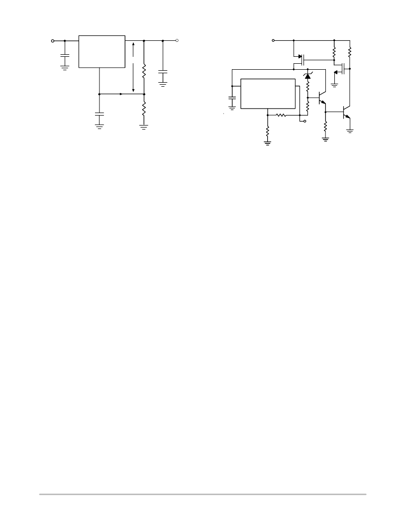
Figure 15. Resistor Divider Scheme
V
REF
R
2
R
1
C
2
V
OUT
V
IN
C
1
V
IN
V
OUT
Adj
NCP1086
The adjustable output linear regulator has an absolute
maximum specification of 7.0 V for the voltage difference
between V
IN
and V
OUT
. However, the IC may be used to
regulate voltages in excess of 7.0 V. The main
considerations in such a design are powerup and short circuit
capability.
In most applications, rampup of the power supply to V
IN
is fairly slow, typically on the order of several tens of
milliseconds, while the regulator responds in less than one
microsecond. In this case, the linear regulator begins
charging the load as soon as the V
IN
to V
OUT
differential is
large enough that the pass transistor conducts current. The
load at this point is essentially at ground, and the supply
voltage is on the order of several hundred mV, with the result
that the pass transistor is in dropout. As the supply to V
IN
increases, the pass transistor will remain in dropout, and
current is passed to the load until V
OUT
reaches the point at
which the IC is in regulation. Further increase in the supply
voltage brings the pass transistor out of dropout. The result
is that the output voltage follows the power supply rampup,
staying in dropout until the regulation point is reached. In
this manner, any output voltage may be regulated. There is
no theoretical limit to the regulated voltage as long as the
V
IN
to V
OUT
differential of 7.0 V is not exceeded.
However, the possibility of destroying the IC in a short
circuit condition is very real for this type of design. Short
circuit conditions will result in the immediate operation of
the pass transistor outside of its safe operating area.
Overvoltage stresses will then cause destruction of the pass
transistor before overcurrent or thermal shutdown circuitry
can become active. Additional circuitry may be required to
clamp the V
IN
to V
OUT
differential to less than 7.0 V if
failsafe operation is required. One possible clamp circuit is
illustrated in Figure 16; however, the design of clamp
circuitry must be done on an application by application
basis. Care must be taken to ensure the clamp actually
protects the design. Components used in the clamp design
must be able to withstand the short circuit condition
indefinitely while protecting the IC.
Figure 16. Short Circuit Protection Circuit for High
Voltage Application
V
IN
V
OUT
Adj
NCP1086
V
OUT
EXTERNAL
SUPPLY
Stability Considerations
The output or compensation capacitor helps determine
three main characteristics of a linear regulator: startup delay,
load transient response and loop stability.
The capacitor value and type is based on cost, availability,
size and temperature constraints. A tantalum or aluminum
electrolytic capacitor is best, since a film or ceramic
capacitor with almost zero ESR can cause instability. The
aluminum electrolytic capacitor is the least expensive
solution. However, when the circuit operates at low
temperatures, both the value and ESR of the capacitor will
vary considerably. The capacitor manufacturers’ data sheet
provides this information.
A 22 F tantalum capacitor will work for most
applications, but with high current regulators such as the
NCP1086 series the transient response and stability improve
with higher values of capacitance. The majority of
applications for this regulator involve large changes in load
current, so the output capacitor must supply the
instantaneous load current. The ESR of the output capacitor
causes an immediate drop in output voltage given by:
V
I
ESR
For microprocessor applications it is customary to use an
output capacitor network consisting of several tantalum and
ceramic capacitors in parallel. This reduces the overall ESR
and reduces the instantaneous output voltage drop under
load transient conditions. The output capacitor network
should be as close as possible to the load for the best results.
相關PDF資料 |
PDF描述 |
|---|---|
| NCP1086T-33 | 1.5 A Adjustable and 3.3 V Fixed Output Linear Regulator |
| NCP1086T-ADJ | 1.5 A Adjustable and 3.3 V Fixed Output Linear Regulator |
| NCP1117DT12G | 1.0 A Low−Dropout Positive Fixed and Adjustable Voltage Regulators |
| NCP1117DT15G | 1.0 A Low−Dropout Positive Fixed and Adjustable Voltage Regulators |
| NCP1117DT18G | 1.0 A Low−Dropout Positive Fixed and Adjustable Voltage Regulators |
相關代理商/技術參數 |
參數描述 |
|---|---|
| NCP1086ST-33T3 | 功能描述:低壓差穩壓器 - LDO 3.3V 1.5A RoHS:否 制造商:Texas Instruments 最大輸入電壓:36 V 輸出電壓:1.4 V to 20.5 V 回動電壓(最大值):307 mV 輸出電流:1 A 負載調節:0.3 % 輸出端數量: 輸出類型:Fixed 最大工作溫度:+ 125 C 安裝風格:SMD/SMT 封裝 / 箱體:VQFN-20 |
| NCP1086ST-33T3G | 功能描述:低壓差穩壓器 - LDO 3.3V 1.5A Commercial Temp RoHS:否 制造商:Texas Instruments 最大輸入電壓:36 V 輸出電壓:1.4 V to 20.5 V 回動電壓(最大值):307 mV 輸出電流:1 A 負載調節:0.3 % 輸出端數量: 輸出類型:Fixed 最大工作溫度:+ 125 C 安裝風格:SMD/SMT 封裝 / 箱體:VQFN-20 |
| NCP1086ST-ADJT3 | 功能描述:低壓差穩壓器 - LDO 1.25-5.5V ADJ 1.5A RoHS:否 制造商:Texas Instruments 最大輸入電壓:36 V 輸出電壓:1.4 V to 20.5 V 回動電壓(最大值):307 mV 輸出電流:1 A 負載調節:0.3 % 輸出端數量: 輸出類型:Fixed 最大工作溫度:+ 125 C 安裝風格:SMD/SMT 封裝 / 箱體:VQFN-20 |
| NCP1086ST-ADJT3G | 功能描述:低壓差穩壓器 - LDO 1.25-5.5V ADJ 1.5A Commercial Temp RoHS:否 制造商:Texas Instruments 最大輸入電壓:36 V 輸出電壓:1.4 V to 20.5 V 回動電壓(最大值):307 mV 輸出電流:1 A 負載調節:0.3 % 輸出端數量: 輸出類型:Fixed 最大工作溫度:+ 125 C 安裝風格:SMD/SMT 封裝 / 箱體:VQFN-20 |
| NCP1086T-033 | 功能描述:低壓差穩壓器 - LDO 3.3V 1.5A RoHS:否 制造商:Texas Instruments 最大輸入電壓:36 V 輸出電壓:1.4 V to 20.5 V 回動電壓(最大值):307 mV 輸出電流:1 A 負載調節:0.3 % 輸出端數量: 輸出類型:Fixed 最大工作溫度:+ 125 C 安裝風格:SMD/SMT 封裝 / 箱體:VQFN-20 |
發布緊急采購,3分鐘左右您將得到回復。