- 您現在的位置:買賣IC網 > PDF目錄361090 > NCP1117DT33G (ON SEMICONDUCTOR) 1.0 A Low−Dropout Positive Fixed and Adjustable Voltage Regulators PDF資料下載
參數資料
| 型號: | NCP1117DT33G |
| 廠商: | ON SEMICONDUCTOR |
| 元件分類: | 基準電壓源/電流源 |
| 英文描述: | 1.0 A Low−Dropout Positive Fixed and Adjustable Voltage Regulators |
| 中文描述: | 3.3 V FIXED POSITIVE LDO REGULATOR, 1.2 V DROPOUT, PSSO2 |
| 封裝: | LEAD FREE, DPAK-3 |
| 文件頁數: | 3/17頁 |
| 文件大小: | 178K |
| 代理商: | NCP1117DT33G |
NCP1117, NCV1117
http://onsemi.com
3
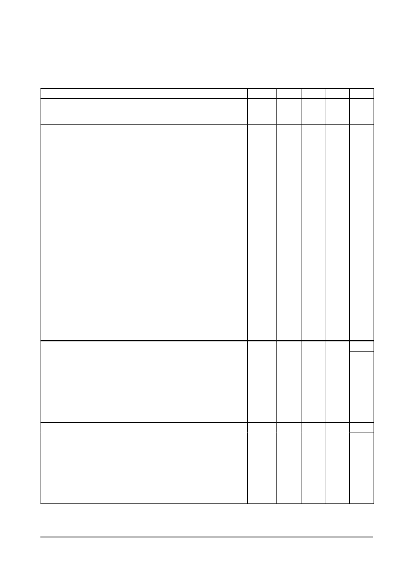
ELECTRICAL CHARACTERISTICS
(C
in
= 10 F, C
out
= 10 F, for typical value T
A
= 25
°
C, for min and max values T
A
is the
operating ambient temperature range that applies unless otherwise noted. (Note 4)
Characteristic
Symbol
Min
Typ
Max
Unit
Reference Voltage, Adjustable Output Devices
(V
in
–V
out
= 2.0 V, I
out
= 10 mA, T
A
= 25
°
C)
(V
in
–V
out
= 1.4 V to 10 V, I
out
= 10 mA to 800 mA) (Note 4)
V
ref
1.238
1.225
1.25
1.262
1.270
V
Output Voltage, Fixed Output Devices
1.5 V
(V
in
= 3.5 V, I
out
= 10 mA, T
A
= 25
°
C)
(V
in
= 2.9 V to 11.5 V, I
out
= 0 mA to 800 mA) (Note 4)
1.8 V
(V
in
= 3.8 V, I
out
= 10 mA, T
A
= 25
°
C)
(V
in
= 3.2 V to 11.8 V, I
out
= 0 mA to 800 mA) (Note 4)
1.9 V
(V
in
= 3.9 V, I
out
= 10 mA, T
A
= 25
°
C)
(V
in
= 3.3 V to 11.9 V, I
out
= 0 mA to 800 mA) (Note 4)
2.0 V
(V
in
= 4.0 V, I
out
= 10 mA, T
A
= 25
°
C)
(V
in
= 3.4 V to 12 V, I
out
= 0 mA to 800 mA) (Note 4)
2.5 V
(V
in
= 4.5 V, I
out
= 10 mA, T
A
= 25
°
C)
(V
in
= 3.9 V to 10 V, I
out
= 0 mA to 800 mA,) (Note 4)
2.85 V
(V
in
= 4.85 V, I
out
= 10 mA, T
A
= 25
°
C)
(V
in
= 4.25 V to 10 V, I
out
= 0 mA to 800 mA) (Note 4)
(V
in
= 4.0 V, I
out
= 0 mA to 500 mA) (Note 5)
3.3 V
(V
in
= 5.3 V, I
out
= 10 mA, T
A
= 25
°
C)
(V
in
= 4.75 V to 10 V, I
out
= 0 mA to 800 mA) (Note 4)
5.0 V
(V
in
= 7.0 V, I
out
= 10 mA, T
A
= 25
°
C)
(V
in
= 6.5 V to 12 V, I
out
= 0 mA to 800 mA) (Note 4)
12 V
(V
in
= 14 V, I
out
= 10 mA, T
A
= 25
°
C)
(V
in
= 13.5 V to 20 V, I
out
= 0 mA to 800 mA) (Note 4)
V
out
1.485
1.470
1.782
1.755
1.872
1.862
1.970
1.960
2.475
2.450
2.821
2.790
2.790
3.267
3.235
4.950
4.900
11.880
11.760
1.500
1.800
1.900
1.900
2.000
2.500
2.850
3.300
5.000
12.000
1.515
1.530
1.818
1.845
1.929
1.938
2.030
2.040
2.525
2.550
2.879
2.910
2.910
3.333
3.365
5.050
5.100
12.120
12.240
V
Line Regulation (Note 5)
Adjustable (V
in
= 2.75 V to 16.25 V, I
out
= 10 mA)
Reg
line
0.04
0.1
%
1.5 V
1.8 V
1.9 V
2.0 V
2.5 V
2.85 V
3.3 V
5.0 V
12 V
(V
in
= 2.9 V to 11.5 V, I
out
= 0 mA)
(V
in
= 3.2 V to 11.8 V, I
out
= 0 mA)
(V
in
= 3.3 V to 11.9 V, I
out
= 0 mA)
(V
in
= 3.4 V to 12 V, I
out
= 0 mA)
(V
in
= 3.9 V to 10 V, I
out
= 0 mA)
(V
in
= 4.25 V to 10 V, I
out
= 0 mA)
(V
in
= 4.75 V to 15 V, I
out
= 0 mA)
(V
in
= 6.5 V to 15 V, I
out
= 0 mA)
(V
in
= 13.5 V to 20 V, I
out
= 0 mA)
0.3
0.4
0.5
0.5
0.5
0.8
0.8
0.9
1.0
1.0
1.0
2.5
2.5
2.5
3.0
4.5
6.0
7.5
mV
Load Regulation (Note 5)
Adjustable (I
out
= 10 mA to 800 mA, V
in
= 4.25 V)
Reg
line
0.2
0.4
%
1.5 V
1.8 V
1.9 V
2.0 V
2.5 V
2.85 V
3.3 V
5.0 V
12 V
(I
out
= 0 mA to 800 mA, V
in
= 2.9 V)
(I
out
= 0 mA to 800 mA, V
in
= 3.2 V)
(I
out
= 0 mA to 800 mA, V
in
= 3.3 V)
(I
out
= 0 mA to 800 mA, V
in
= 3.4 V)
(I
out
= 0 mA to 800 mA, V
in
= 3.9 V)
(I
out
= 0 mA to 800 mA, V
in
= 4.25 V)
(I
out
= 0 mA to 800 mA, V
in
= 4.75 V)
(I
out
= 0 mA to 800 mA, V
in
= 6.5 V)
(I
out
= 0 mA to 800 mA, V
in
= 13.5 V)
2.3
2.6
2.7
3.0
3.3
3.8
4.3
6.7
16
5.5
6.0
6.0
6.0
7.5
8.0
10
15
28
mV
4. The regulator output current must not exceed 1.0 A with V
greater than 12 V.
5. Low duty cycle pulse techniques are used during testing to maintain the junction temperature as close to ambient as possible.
相關PDF資料 |
PDF描述 |
|---|---|
| NCP1117DT50G | 1.0 A Low−Dropout Positive Fixed and Adjustable Voltage Regulators |
| NCP1117DTAT5G | 1.0 A Low−Dropout Positive Fixed and Adjustable Voltage Regulators |
| NCP1117ST12T3G | 1.0 A Low−Dropout Positive Fixed and Adjustable Voltage Regulators |
| NCP1117ST285T3G | 1.0 A Low−Dropout Positive Fixed and Adjustable Voltage Regulators |
| NCP1117ST50T3G | 1.0 A Low−Dropout Positive Fixed and Adjustable Voltage Regulators |
相關代理商/技術參數 |
參數描述 |
|---|---|
| NCP1117DT33G | 制造商:ON Semiconductor 功能描述:Voltage Regulator IC |
| NCP1117DT33RK | 功能描述:低壓差穩壓器 - LDO 3.3V 1A Positive RoHS:否 制造商:Texas Instruments 最大輸入電壓:36 V 輸出電壓:1.4 V to 20.5 V 回動電壓(最大值):307 mV 輸出電流:1 A 負載調節:0.3 % 輸出端數量: 輸出類型:Fixed 最大工作溫度:+ 125 C 安裝風格:SMD/SMT 封裝 / 箱體:VQFN-20 |
| NCP1117DT33RKG | 功能描述:低壓差穩壓器 - LDO 3.3V 1A Positive RoHS:否 制造商:Texas Instruments 最大輸入電壓:36 V 輸出電壓:1.4 V to 20.5 V 回動電壓(最大值):307 mV 輸出電流:1 A 負載調節:0.3 % 輸出端數量: 輸出類型:Fixed 最大工作溫度:+ 125 C 安裝風格:SMD/SMT 封裝 / 箱體:VQFN-20 |
| NCP1117DT33RKG | 制造商:ON Semiconductor 功能描述:Linear Voltage Regulator IC |
| NCP1117DT33RKG-CUT TAPE | 制造商:ON 功能描述:NCP1117 Series 3.3 V 1 A Low-Dropout Positive Fixed Voltage Regulator-DPAK-3 |
發布緊急采購,3分鐘左右您將得到回復。