- 您現在的位置:買賣IC網 > PDF目錄361091 > NCP1337 (ON SEMICONDUCTOR) PWM Current−Mode Controller for Free Running Quasi−Resonant Operation PDF資料下載
參數資料
| 型號: | NCP1337 |
| 廠商: | ON SEMICONDUCTOR |
| 英文描述: | PWM Current−Mode Controller for Free Running Quasi−Resonant Operation |
| 文件頁數: | 11/14頁 |
| 文件大小: | 148K |
| 代理商: | NCP1337 |
NCP1337
http://onsemi.com
11
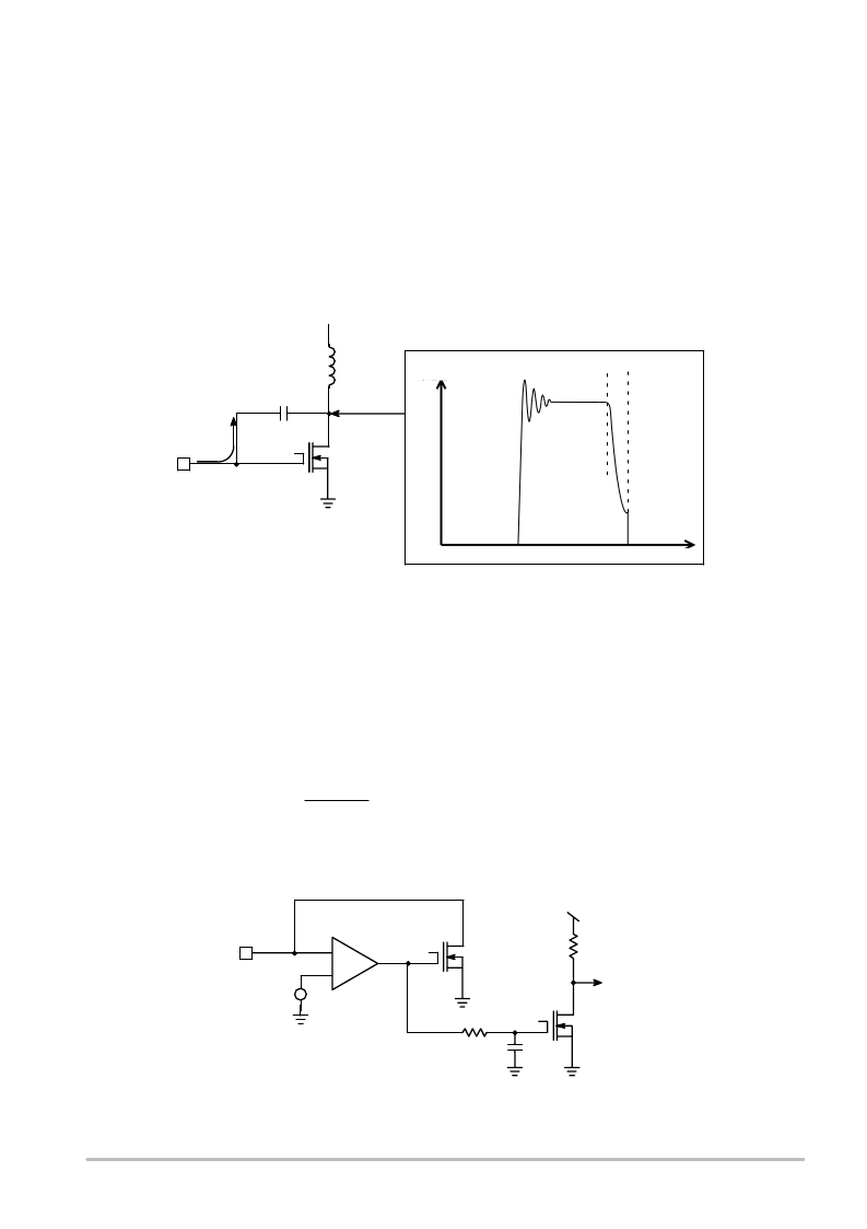
Soxyless
The “Valley point detection” is based on the observation
of the Power MOSFET Drain voltage variations. When the
transformer is fully demagnetized, the Drain voltage
evolution from the plateau level down to the V
IN
asymptote
is governed by the resonating energy transfer between the
L
P
transformer inductor and the global capacitance present
on the Drain. These voltage oscillations create current
oscillation in the parasitic capacitor across the switching
MOSFET (modelized by the Crss capacitance between
Gate and Drain): a negative current (flowing out of DRV
pin) takes place during the decreasing part of the Drain
oscillation, and a positive current (entering into the DRV
pin) during the increasing part.
The Drain valley corresponds to the inversion of the
current (i.e., the zero crossing): by detecting this point, we
always ensure a true valley turnon.
Lprim
Crss
DRV
Isoxy
Vswitch
T
SWING
t
Figure 6. Soxyless Concept
The current in the Power MOSFET gate is:
Igate = Vringing/Zc (with Zc the capacitance impedance)
so
Igate = Vringing (2 Fres Crss)
The magnitude of this gate current depends on the
MOSFET, the resonating frequency and the voltage swing
present on the Drain at the end of the plateau voltage.
The dead time T
SWING
is given by the equation:
Tswing
0.5 Fres
* Lp * Cdrain
(eq. 1)
(where L
P
is the primary transformer inductance and
C
DRAIN
the total capacitance present on the MOSFET
Drain. This capacitance includes the snubber capacitor if
any, the transformer windings stray capacitance plus the
parasitic MOSFET capacitances C
OSS
and C
RSS
).
Internal Feedback Circuitry
To simplify the implementation of a primary regulation,
it is necessary to inject a current into the FB pin (instead of
sourcing it out). But to have a precise primary regulation,
the voltage present on FB pin must be regulated. Figure 8
gives the FB pin internal implementation: the circuitry
combines the functions of a current to voltage converter
and a voltage regulator.
FB
+
+
3 V
Vdd
Internal
Setpoint
20 kHz
Lowpass Filter
Figure 7. Internal Implementation of FB Pin
相關PDF資料 |
PDF描述 |
|---|---|
| NCP1337DR2G | PWM Current−Mode Controller for Free Running Quasi−Resonant Operation |
| NCP1337PG | PWM Current−Mode Controller for Free Running Quasi−Resonant Operation |
| NCP1351 | Variable Off Time PWM Controller |
| NCP1351ADR2G | Variable Off Time PWM Controller |
| NCP1351BDR2G | Variable Off Time PWM Controller |
相關代理商/技術參數 |
參數描述 |
|---|---|
| NCP1337_11 | 制造商:ONSEMI 制造商全稱:ON Semiconductor 功能描述:PWM Current-Mode Controller for Free Running Quasi-Resonant Operation |
| NCP1337ADAPEVB | 功能描述:插座和適配器 NCP1337 60W ADAPTER EVB RoHS:否 制造商:Silicon Labs 產品:Adapter 用于:EM35x |
| NCP1337ADAPGEVB | 功能描述:電源管理IC開發工具 NCP1337 60W ADAPTER EVB RoHS:否 制造商:Maxim Integrated 產品:Evaluation Kits 類型:Battery Management 工具用于評估:MAX17710GB 輸入電壓: 輸出電壓:1.8 V |
| NCP1337DR2G | 功能描述:電流型 PWM 控制器 PWM CONTROLLER RoHS:否 制造商:Texas Instruments 開關頻率:27 KHz 上升時間: 下降時間: 工作電源電壓:6 V to 15 V 工作電源電流:1.5 mA 輸出端數量:1 最大工作溫度:+ 105 C 安裝風格:SMD/SMT 封裝 / 箱體:TSSOP-14 |
| NCP1337PG | 功能描述:電流型 PWM 控制器 PWM CONTROLLER RoHS:否 制造商:Texas Instruments 開關頻率:27 KHz 上升時間: 下降時間: 工作電源電壓:6 V to 15 V 工作電源電流:1.5 mA 輸出端數量:1 最大工作溫度:+ 105 C 安裝風格:SMD/SMT 封裝 / 箱體:TSSOP-14 |
發布緊急采購,3分鐘左右您將得到回復。