- 您現在的位置:買賣IC網 > PDF目錄361091 > NCP1351 (ON SEMICONDUCTOR) Variable Off Time PWM Controller PDF資料下載
參數資料
| 型號: | NCP1351 |
| 廠商: | ON SEMICONDUCTOR |
| 英文描述: | Variable Off Time PWM Controller |
| 中文描述: | 變關閉時間PWM控制器 |
| 文件頁數: | 15/19頁 |
| 文件大小: | 222K |
| 代理商: | NCP1351 |
NCP1351
http://onsemi.com
15
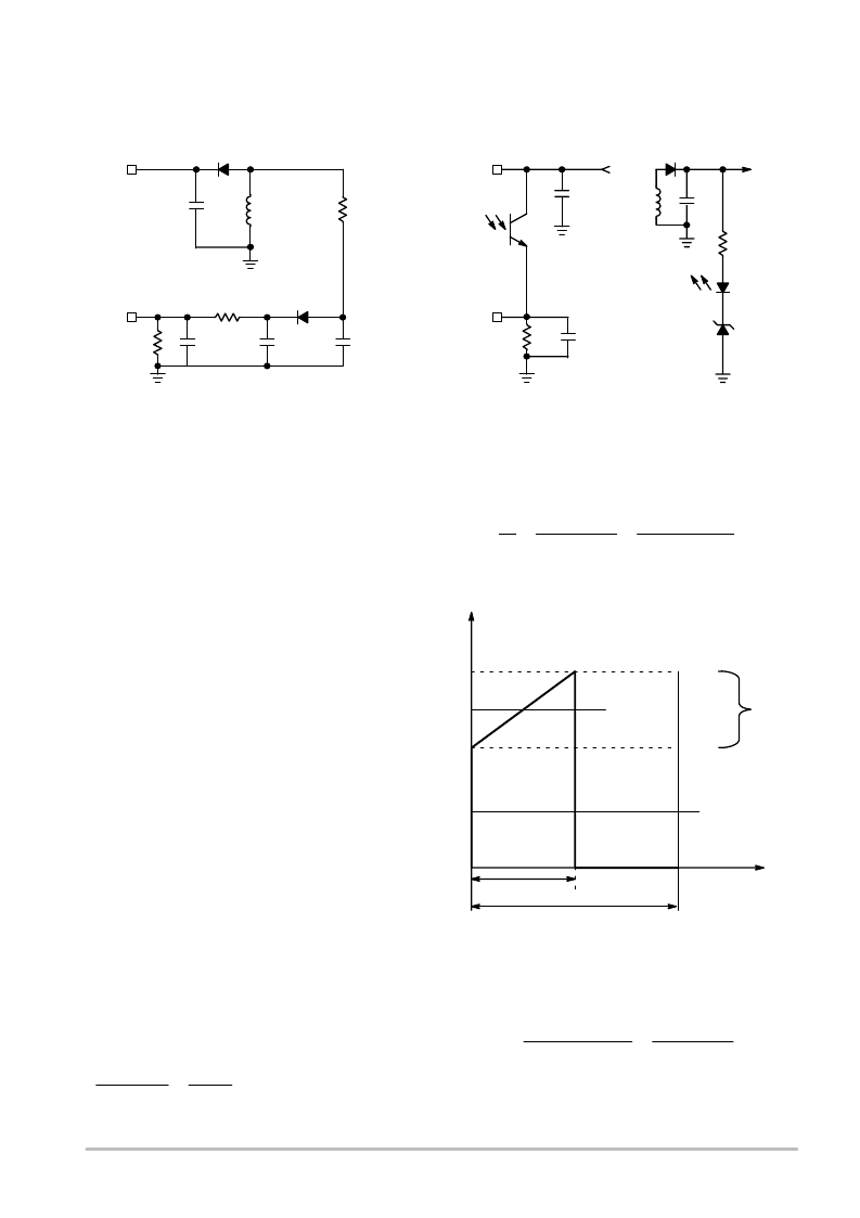
Figure 19. You can either directly observe the V
CC
level or add a small RC filter to reduce the leakage inductance
contribution. The best is to directly sense the output voltage and reacts if it runs away, as offered on the right
side.
C4
100n
R4
2.2k
C5
1n
V
CC
Latch
100nF
L
aux
R
OVP
D2
1N4937
R
pulldown
CV
CC
20 F
V
CC
Latch
C3
C1
100nF
Aux
Sec
U1A
D4
OUT
CV
CC
22 F
U1B
+
+
Design Example, a 19 V / 3
A Universal Mains Power Supply Designing a
SwitchMode Power Supply using the NCP1351 does not
differ from a fixed frequency design. What changes,
however, is the regulation method via frequency variations.
In other words, all the calculations must be carried at the
lowest line input where the frequency will hit the maximum
value set by the C
t
capacitor. Let us follow the steps:
V
in
min = 100 Vdc (bulk valley in lowline conditions)
V
in
max = 375 Vdc
V
out
= 19 V
I
out
= 3 A
Operating mode is CCM
η
= 0.8
F
sw
= 65 kHz
1. Turn Ratio. This is the first parameter to consider.
The MOSFET BV
dss
actually dictates the amount
of reflected voltage you need. If we consider a
600 V MOSFET and a 15% derating factor, we
must limit the maximum drain voltage to:
Vds_max
600
0.85
510 V
(eq. 16)
Knowing a maximum bulk voltage of 375 V, the clamp
voltage must be set to:
Vclamp
510
375
135 V
(eq. 17)
Based on the above level, we decide to adopt a headroom
between the reflected voltage and the clamp level of 50 V. If
this headroom is too small, a high dissipation will occur on
the RDC clamp network and efficiency will suffer. A
leakage inductance of around 1% of the magnetizing value
should give good results with this choice (k
c
= 1.6). The turn
ratio between primary and secondary is simply:
Vout
V
f
N
Vclamp
kc
(eq. 18)
Solving for N gives:
N
Ns
Np
0.234
kCVout
Vclamp
V
f
1.6
(19
135
0.8)
(eq. 19)
Let us round it to 0.25 or 1/N = 4
Figure 20. Primary Inductance Current Evolution
in CCM
DT
SW
I
L
T
SW
I
peak
I
valley
I
avg
I
1
t
2. Calculate the maximum operating dutycycle for
this flyback converter operated in CCM:
VoutN
VoutN
Vin_min
dmax
19
4
19
4
100
0.43
(eq. 20)
相關PDF資料 |
PDF描述 |
|---|---|
| NCP1351ADR2G | Variable Off Time PWM Controller |
| NCP1351BDR2G | Variable Off Time PWM Controller |
| NCP1381 | Low−Standby High Performance PWM Controller |
| NCP1381DR2G | Low−Standby High Performance PWM Controller |
| NCP1395APG | High Performance Resonant Mode Controller |
相關代理商/技術參數 |
參數描述 |
|---|---|
| NCP1351ADAPGEVB | 功能描述:電源管理IC開發工具 NCP1351 57 W ADAPTER EVB RoHS:否 制造商:Maxim Integrated 產品:Evaluation Kits 類型:Battery Management 工具用于評估:MAX17710GB 輸入電壓: 輸出電壓:1.8 V |
| NCP1351ADR2G | 功能描述:電流型 PWM 控制器 OSPI PWM CONTROLLER RoHS:否 制造商:Texas Instruments 開關頻率:27 KHz 上升時間: 下降時間: 工作電源電壓:6 V to 15 V 工作電源電流:1.5 mA 輸出端數量:1 最大工作溫度:+ 105 C 安裝風格:SMD/SMT 封裝 / 箱體:TSSOP-14 |
| NCP1351APG | 功能描述:電流型 PWM 控制器 VRIABLE OFF TM CNTRL RoHS:否 制造商:Texas Instruments 開關頻率:27 KHz 上升時間: 下降時間: 工作電源電壓:6 V to 15 V 工作電源電流:1.5 mA 輸出端數量:1 最大工作溫度:+ 105 C 安裝風格:SMD/SMT 封裝 / 箱體:TSSOP-14 |
| NCP1351BDR2G | 功能描述:電流型 PWM 控制器 OSPI PWM CONTROLLER RoHS:否 制造商:Texas Instruments 開關頻率:27 KHz 上升時間: 下降時間: 工作電源電壓:6 V to 15 V 工作電源電流:1.5 mA 輸出端數量:1 最大工作溫度:+ 105 C 安裝風格:SMD/SMT 封裝 / 箱體:TSSOP-14 |
| NCP1351BPG | 功能描述:電流型 PWM 控制器 VRIABLE OFF TM CNTRL RoHS:否 制造商:Texas Instruments 開關頻率:27 KHz 上升時間: 下降時間: 工作電源電壓:6 V to 15 V 工作電源電流:1.5 mA 輸出端數量:1 最大工作溫度:+ 105 C 安裝風格:SMD/SMT 封裝 / 箱體:TSSOP-14 |
發布緊急采購,3分鐘左右您將得到回復。