- 您現在的位置:買賣IC網 > PDF目錄361092 > NCP1411 (ON SEMICONDUCTOR) Sync-Rect PFM Step-Up DC-DC Converter(帶有同步整流器的PFM升壓DC-DC轉換器) PDF資料下載
參數資料
| 型號: | NCP1411 |
| 廠商: | ON SEMICONDUCTOR |
| 元件分類: | DC/DC變換器 |
| 英文描述: | Sync-Rect PFM Step-Up DC-DC Converter(帶有同步整流器的PFM升壓DC-DC轉換器) |
| 中文描述: | 同步整流PFM型升壓型DC - DC轉換器(帶有同步整流器的烤瓷升壓型DC - DC轉換器) |
| 文件頁數: | 2/14頁 |
| 文件大小: | 358K |
| 代理商: | NCP1411 |
NCP1411
http://onsemi.com
2
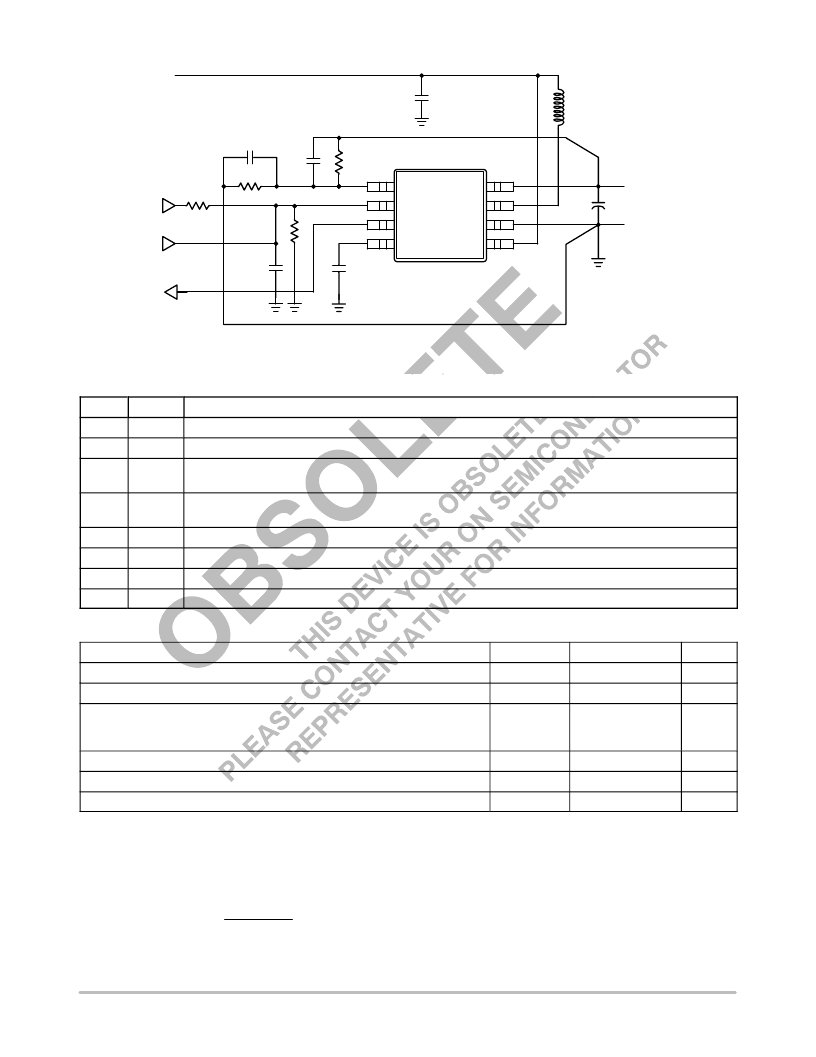
Figure 1. Typical Operating Circuit
FB
LBI/EN
LBO
REF
OUT
LX
GND
BAT
4
3
2
1
5
6
7
8
150 nF
33 F
NCP1411
+
350 k
10 F
22 H
220 pF
150 pF
200 k
C
EN
120 nF
Output 1.5 to 5.5 V
I
OUT
Typical
Up to 250 mA at
3.3 V Output
and 2.5 V Input
Input
1 V to
V
OUT
Low Battery
Sense Input
Shutdown
Open Drain
Input
Low Battery
Open Drain
Output
R
LB1
R
LB2
ááááááááááááááááááááááááááááááááá
ááááááááááááááááááááááááááááááááá
ááááááááááááááááááááááááááááááááá
FB
Output Voltage Feedback Input.
2
LBI/EN
Low
Battery Detector Input and IC Enable.
3
LBO
Open
Drain Low
Battery Detector Output. Output is LOW when V
LBI
is < 1.178 V. LBO is high impedance during
shutdown.
4
REF
1.190 V Reference Voltage Output, bypassing with 150 nF capacitor if this pin is not loaded, bypassing with 1.0 F
if this pin is loaded up to 2.5 mA @ V
OUT
= 3.3 V.
5
BAT
Battery input connection for internal Ring
Killer.
6
GND
Ground.
7
LX
N
Channel and P
Channel Power MOSFET Drain Connection.
8
OUT
Power Output. OUT also provides bootstrapped power to the device.
MAXIMUM RATINGS
Rating
Symbol
Value
Unit
Device Power Supply (Pin 8)
V
OUT
0.3 to 6.0
V
Input/Output Pins (Pins 1
5, Pin 7)
V
IO
0.3 to 6.0
V
Thermal Characteristics
Micro8 Plastic Package
Maximum Power Dissipation @ T
A
= 25
°
C
Thermal Resistance, Junction
to
Air
P
D
R
JA
520
240
mW
°
C/W
Operating Junction Temperature Range
T
J
40 to +150
°
C
Operating Ambient Temperature Range
T
A
40 to +85
°
C
Storage Temperature Range
T
stg
55 to +150
°
C
Stresses exceeding Maximum Ratings may damage the device. Maximum Ratings are stress ratings only. Functional operation above the
Recommended Operating Conditions is not implied. Extended exposure to stresses above the Recommended Operating Conditions may affect
device reliability.
1. This device contains ESD protection and exceeds the following tests:
Human Body Model (HBM)
2.0 kV per JEDEC standard: JESD22
A114.
Machine Model (MM)
200 V per JEDEC standard: JESD22
A115.
2. The maximum package power dissipation limit must not be exceeded.
TJ(max)
TA
RJA
3. Latchup Current Maximum Rating:
150 mA per JEDEC standard: JESD78.
4. Moisture Sensitivity Level: MSL 1 per IPC/JEDEC standard: J
STD
020A.
PD
相關PDF資料 |
PDF描述 |
|---|---|
| NCP1417DMR2(中文) | 200 mA DC-DC Step-up Converter with Dual Low Battery Protection(帶雙路低電池保護的200mA步升DC-DC轉換器) |
| NCP1417 | 200 mA DC-DC Step-up Converter with Dual Low Battery Protection |
| NCP1417DMR2 | 200 mA DC-DC Step-up Converter with Dual Low Battery Protection |
| NCP1421DMR2(中文) | 600 mA Sync-Rect PFM Step-Up DC-DC Converter with True-Cutoff and Ring-Killer(帶真切斷(true-cutoff)和振蕩消除(ring-killer)的600mA同步整流PFM步升DC-DC 轉換器) |
| NCP1421DMR2 | 600 mA Sync-Rect PFM Step-Up DC-DC Converter Step-Up DC-DC Converter with True-Cutoff and Ring-Killer |
相關代理商/技術參數 |
參數描述 |
|---|---|
| NCP1411DMR2 | 功能描述:直流/直流開關轉換器 250mA Monolithic RoHS:否 制造商:STMicroelectronics 最大輸入電壓:4.5 V 開關頻率:1.5 MHz 輸出電壓:4.6 V 輸出電流:250 mA 輸出端數量:2 最大工作溫度:+ 85 C 安裝風格:SMD/SMT |
| NCP1411DMR2G | 功能描述:直流/直流開關轉換器 250mA Monolithic High Frequency Boost RoHS:否 制造商:STMicroelectronics 最大輸入電壓:4.5 V 開關頻率:1.5 MHz 輸出電壓:4.6 V 輸出電流:250 mA 輸出端數量:2 最大工作溫度:+ 85 C 安裝風格:SMD/SMT |
| NCP1417DMR2 | 功能描述:直流/直流開關轉換器 200mA DC/DC Boost RoHS:否 制造商:STMicroelectronics 最大輸入電壓:4.5 V 開關頻率:1.5 MHz 輸出電壓:4.6 V 輸出電流:250 mA 輸出端數量:2 最大工作溫度:+ 85 C 安裝風格:SMD/SMT |
| NCP1417-SKT | 制造商:ON Semiconductor 功能描述:Sample Kit, Including 2 NCP1417DM2 and 1 Development Resource CD-ROM 制造商:P&S 功能描述:Sample Kit, Including 2 NCP1417DM2 and 1 Development Resource CD-ROM |
| NCP1421DMR2 | 功能描述:直流/直流開關轉換器 600mA PFM Boost RoHS:否 制造商:STMicroelectronics 最大輸入電壓:4.5 V 開關頻率:1.5 MHz 輸出電壓:4.6 V 輸出電流:250 mA 輸出端數量:2 最大工作溫度:+ 85 C 安裝風格:SMD/SMT |
發布緊急采購,3分鐘左右您將得到回復。