參數資料
| 型號: | NCP4300ADG |
| 廠商: | ON Semiconductor |
| 文件頁數: | 1/7頁 |
| 文件大小: | 0K |
| 描述: | IC OPAMP/VOLTAGE REF DUAL 8-SOIC |
| 標準包裝: | 98 |
| 放大器類型: | 通用 |
| 電路數: | 2 |
| 轉換速率: | 0.5 V/µs |
| 增益帶寬積: | 700kHz |
| 電流 - 輸入偏壓: | 50nA |
| 電壓 - 輸入偏移: | 500µV |
| 電流 - 電源: | 420µA |
| 電流 - 輸出 / 通道: | 25mA |
| 電壓 - 電源,單路/雙路(±): | 3 V ~ 35 V |
| 工作溫度: | 0°C ~ 105°C |
| 安裝類型: | 表面貼裝 |
| 封裝/外殼: | 8-SOIC(0.154",3.90mm 寬) |
| 供應商設備封裝: | 8-SOICN |
| 包裝: | 管件 |
Semiconductor Components Industries, LLC, 2009
August, 2009 Rev. 4
1
Publication Order Number:
NCP4300A/D
NCP4300A
Dual Operational Amplifier
and Voltage Reference
The NCP4300A is a monolithic integrated circuit specifically
designed to control the output current and voltage levels of switch
mode battery chargers and power supplies. This device contains a
precision 2.6 V shunt reference and two operational amplifiers.
OpAmp 1 is designed to perform voltage control and has its
noninverting input internally connected to the reference. OpAmp 2
is designed for current control and has both inputs uncommitted. The
NCP4300A offers the power converter designer a control solution that
features increased precision with a corresponding reduction in system
complexity and cost. This device is available in an 8lead surface
mount package.
Features
This is a PbFree Device
Operational Amplifier
Low Input Offset Voltage: 0.5 mV
Input Common Mode Voltage Range Includes Ground
Low Supply Current: 210 mA/OpAmp (@VCC = 5.0 V)
Medium Unity Gain Bandwidth: 0.7 MHz
Large Output Voltage Swing: 0 V to VCC 1.5 V
Wide Power Supply Voltage Range: 3.0 V to 35 V
Voltage Reference
Fixed Output Voltage Reference: 2.60 V
High Precision Over Temperature: 1.0%
Wide Sink Current Range: 80 mA to 80 mA
Typical Applications
Battery Charger
Switch Mode Power Supply
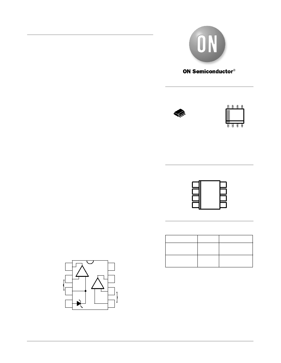
Figure 1. Functional Block Diagram
+
Output 1
Inputs 1
VCC
Output 2
GND
+
1
2
3
4
7
6
5
8
Inputs 2
-
2.6 V
http://onsemi.com
MARKING
DIAGRAM
SOIC8
D SUFFIX
CASE 751
1
8
PIN CONNECTIONS
18
7
6
5
2
3
4
(Top View)
Out 1
In 1
In 1+
VCC
Out 2
In 2+
In 2
GND
A = Assembly Location
L = Wafer Lot
Y = Year
W = Work Week
A = Option Code
G = PbFree Package
Device
Package
Shipping
ORDERING INFORMATION
For information on tape and reel specifications,
including part orientation and tape sizes, please
refer to our Tape and Reel Packaging Specification
Brochure, BRD8011/D.
N4300
ALYWA
G
1
8
NCP4300ADR2G
SOIC8
(PbFree)
2500/Tape & Reel
NCP4300ADG
SOIC8
(PbFree)
98 Units / Rail
相關PDF資料 |
PDF描述 |
|---|---|
| TLC2274CNSR | IC OPAMP GP R-R 2.25MHZ 14SOP |
| 3408-1202 | CONN HEADER 16PS R/A SHORT LATCH |
| 77313-122-10 | HDR STR DR .100 DP |
| TVP06B360CA-G | TVS 600W 36V BIDIRECT SMC |
| TVP06B330CA-G | TVS 600W 33V BIDIRECT SMC |
相關代理商/技術參數 |
參數描述 |
|---|---|
| NCP4300ADR2 | 功能描述:運算放大器 - 運放 2.6V Ref. RoHS:否 制造商:STMicroelectronics 通道數量:4 共模抑制比(最小值):63 dB 輸入補償電壓:1 mV 輸入偏流(最大值):10 pA 工作電源電壓:2.7 V to 5.5 V 安裝風格:SMD/SMT 封裝 / 箱體:QFN-16 轉換速度:0.89 V/us 關閉:No 輸出電流:55 mA 最大工作溫度:+ 125 C 封裝:Reel |
| NCP4300ADR2G | 功能描述:運算放大器 - 運放 2.6V Ref. Dual Op AMP RoHS:否 制造商:STMicroelectronics 通道數量:4 共模抑制比(最小值):63 dB 輸入補償電壓:1 mV 輸入偏流(最大值):10 pA 工作電源電壓:2.7 V to 5.5 V 安裝風格:SMD/SMT 封裝 / 箱體:QFN-16 轉換速度:0.89 V/us 關閉:No 輸出電流:55 mA 最大工作溫度:+ 125 C 封裝:Reel |
| NCP4302 | 制造商:ONSEMI 制造商全稱:ON Semiconductor 功能描述:Secondary Side Synchronous Flyback Controller |
| NCP4302ADR2G | 功能描述:初級與次級側 PWM 控制器 SYNCHRONOUS RECTFICTION CONTRLLR RoHS:否 制造商:ON Semiconductor 輸出端數量:1 開關頻率:250 KHz 工作電源電壓:- 0.3 V to + 28 V 最大工作溫度:+ 85 C 最小工作溫度:- 5 C 封裝 / 箱體:SOIC-8 Narrow 封裝:Reel |
| NCP4302ADR2G | 制造商:ON Semiconductor 功能描述:Off-Line Controller IC |
發布緊急采購,3分鐘左右您將得到回復。