- 您現(xiàn)在的位置:買賣IC網(wǎng) > PDF目錄5606 > NE5517DR2G (ON Semiconductor)IC AMP XCONDUCTANCE DUAL 16-SOIC PDF資料下載
參數(shù)資料
| 型號: | NE5517DR2G |
| 廠商: | ON Semiconductor |
| 文件頁數(shù): | 1/15頁 |
| 文件大小: | 0K |
| 描述: | IC AMP XCONDUCTANCE DUAL 16-SOIC |
| 標準包裝: | 1 |
| 放大器類型: | 跨導 |
| 電路數(shù): | 2 |
| 輸出類型: | 推挽式 |
| 轉換速率: | 50 V/µs |
| 增益帶寬積: | 2MHz |
| 電流 - 輸入偏壓: | 400nA |
| 電壓 - 輸入偏移: | 400µV |
| 電流 - 電源: | 2.6mA |
| 電流 - 輸出 / 通道: | 650µA |
| 電壓 - 電源,單路/雙路(±): | 4 V ~ 44 V,±2 V ~ 22 V |
| 工作溫度: | 0°C ~ 70°C |
| 安裝類型: | 表面貼裝 |
| 封裝/外殼: | 16-SOIC(0.154",3.90mm 寬) |
| 供應商設備封裝: | 16-SOIC |
| 包裝: | 剪切帶 (CT) |
| 其它名稱: | NE5517DR2GOSCT |
Semiconductor Components Industries, LLC, 2013
June, 2013 Rev. 4
1
Publication Order Number:
NE5517/D
NE5517, NE5517A, AU5517
Dual Operational
Transconductance Amplifier
The AU5517 and NE5517 contain two current-controlled
transconductance amplifiers, each with a differential input and
push-pull output. The AU5517/NE5517 offers significant design and
performance advantages over similar devices for all types of
programmable gain applications. Circuit performance is enhanced
through the use of linearizing diodes at the inputs which enable a
10 dB signal-to-noise improvement referenced to 0.5% THD. The
AU5517/NE5517 is suited for a wide variety of industrial and
consumer applications.
Constant impedance of the buffers on the chip allow general use of
the AU5517/NE5517. These buffers are made of Darlington
transistors and a biasing network that virtually eliminate the change of
offset voltage due to a burst in the bias current IABC, hence eliminating
the audible noise that could otherwise be heard in high quality audio
applications.
Features
Constant Impedance Buffers
DVBE of Buffer is Constant with Amplifier IBIAS Change
Excellent Matching Between Amplifiers
Linearizing Diodes
High Output Signal-to-Noise Ratio
PbFree Packages are Available*
Applications
Multiplexers
Timers
Electronic Music Synthesizers
Dolby HX Systems
Current-Controlled Amplifiers, Filters
Current-Controlled Oscillators, Impedances
*For additional information on our PbFree strategy and soldering details, please
download the ON Semiconductor Soldering and Mounting Techniques
Reference Manual, SOLDERRM/D.
http://onsemi.com
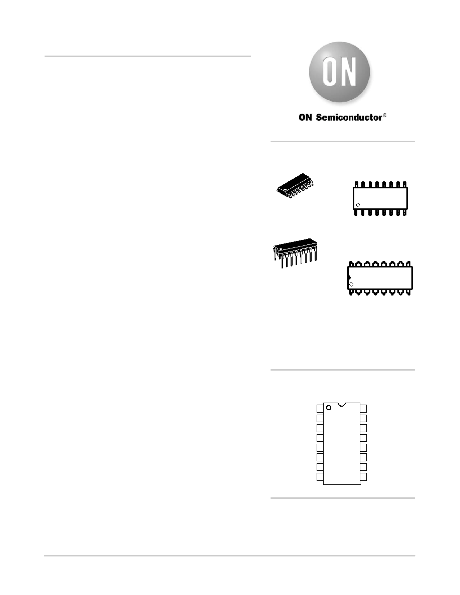
PIN CONNECTIONS
See detailed ordering and shipping information in the package
dimensions section on page 13 of this data sheet.
ORDERING INFORMATION
1
2
3
4
5
6
7
8
9
10
11
12
13
14
16
15
IABCa
Da
+INa
INa
VOa
V
INBUFFERa
VOBUFFERa
IABCb
Db
+INb
INb
VOb
V+
INBUFFERb
VOBUFFERb
N, D Packages
(Top View)
PDIP16
N SUFFIX
CASE 648
1
SOIC16
D SUFFIX
CASE 751B
1
MARKING
DIAGRAMS
NE5517yy
AWLYYWWG
xx
= AU or NE
yy
= AN or N
A
= Assembly Location
WL
= Wafer Lot
YY, Y = Year
WW = Work Week
G
= PbFree Package
xx5517DG
AWLYWW
1
相關PDF資料 |
PDF描述 |
|---|---|
| FWJ-18-01-T-S | CONN HEADER .156" 18POS SNGL TIN |
| 929648-01-36-I | CONN HEADER 36POS R/A .100" GOLD |
| CRCW04024R87FKED | RES 4.87 OHM 1/16W 1% 0402 SMD |
| SMS24CT1G | TVS ARRAY 5LINE 350W SC74-6 |
| NCV33274ADR2G | IC OPAMP QUAD HS BIPO 14-SOIC |
相關代理商/技術參數(shù) |
參數(shù)描述 |
|---|---|
| NE5517D-T | 制造商:未知廠家 制造商全稱:未知廠家 功能描述:Transconductance Operational Amplifier |
| NE5517N | 功能描述:跨導放大器 Transconductance RoHS:否 制造商:Texas Instruments 通道數(shù)量:1 封裝 / 箱體:SOIC-14 帶寬: 輸入補償電壓:40 mV at +/- 5 V 電源電壓-最大:+/- 5 V 電源電流: 最大工作溫度:+ 85 C 最小工作溫度:- 40 C 封裝:Tube |
| NE5517NG | 功能描述:跨導放大器 Transconductance Dual Commercial Temp RoHS:否 制造商:Texas Instruments 通道數(shù)量:1 封裝 / 箱體:SOIC-14 帶寬: 輸入補償電壓:40 mV at +/- 5 V 電源電壓-最大:+/- 5 V 電源電流: 最大工作溫度:+ 85 C 最小工作溫度:- 40 C 封裝:Tube |
| NE5520279A | 功能描述:射頻MOSFET電源晶體管 L/S Band Med Power RoHS:否 制造商:Freescale Semiconductor 配置:Single 晶體管極性: 頻率:1800 MHz to 2000 MHz 增益:27 dB 輸出功率:100 W 汲極/源極擊穿電壓: 漏極連續(xù)電流: 閘/源擊穿電壓: 最大工作溫度: 封裝 / 箱體:NI-780-4 封裝:Tray |
| NE5520279A-A | 功能描述:射頻MOSFET電源晶體管 L/S Band Med Power RoHS:否 制造商:Freescale Semiconductor 配置:Single 晶體管極性: 頻率:1800 MHz to 2000 MHz 增益:27 dB 輸出功率:100 W 汲極/源極擊穿電壓: 漏極連續(xù)電流: 閘/源擊穿電壓: 最大工作溫度: 封裝 / 箱體:NI-780-4 封裝:Tray |
發(fā)布緊急采購,3分鐘左右您將得到回復。