- 您現在的位置:買賣IC網 > PDF目錄361113 > NE699M01-T1 (NEC Corp.) NPN EPITAXIAL SILICON TRANSISTOR FOR MICROWAVE HIGH-GAIN AMPLIFICATION PDF資料下載
參數資料
| 型號: | NE699M01-T1 |
| 廠商: | NEC Corp. |
| 英文描述: | NPN EPITAXIAL SILICON TRANSISTOR FOR MICROWAVE HIGH-GAIN AMPLIFICATION |
| 中文描述: | npn型外延硅晶體管的微波高增益放大 |
| 文件頁數: | 1/6頁 |
| 文件大小: | 50K |
| 代理商: | NE699M01-T1 |
PART NUMBER
PACKAGE OUTLINE
NE699M01
M01
SYMBOLS
PARAMETERS AND CONDITIONS
UNITS
MIN
TYP
MAX
I
CBO
I
EBO
h
FE1
f
T
C
RE2
|S
21E
|
2
NF
Collector Cutoff Current at V
CB
= 5 V, I
E
= 0
Emitter Cutoff Current at V
EB
= 1 V, I
C
= 0
DC Current Gain at V
CE
= 2 V, I
C
= 20 mA
Gain Bandwidth Product at V
CE
= 2 V, I
C
= 20mA, f = 2.0GHz
Feedback Capacitance at V
CB
= 2 V, I
E
= 0, f = 1 MHz
Insertion Power Gain at V
CE
= 2 V, I
C
= 20 mA, f = 2.0 GHz
Noise Figure at V
CE
= 2 V, I
C
= 3 mA, f = 2.0 GHz
μ
A
μ
A
0.1
0.1
140
70
13
GHz
pF
dB
dB
16
0.2
14
1.1
0.3
12
1.8
NE699M01
NPN EPITAXIAL SILICON
TRANSISTOR FOR MICROWAVE
HIGH-GAIN AMPLIFICATION
HIGH f
T
:
16 GHz TYP at 2 V, 20 mA
LOW NOISE FIGURE:
NF = 1.1 dB TYP at 2 GHz
HIGH GAIN:
|S
21E
|
2
= 14 dB TYP at f =
2 GHz
6 PIN SMALL MINI MOLD PACKAGE
EXCELLENT LOW VOLTAGE,
LOW CURRENT PERFORMANCE
FEATURES
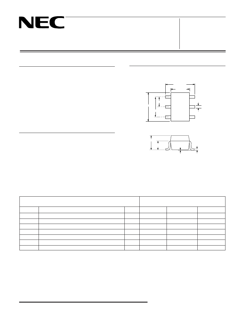
OUTLINE DIMENSIONS
(Units in mm)
PACKAGE OUTLINE M01
DESCRIPTION
PRELIMINARY DATA SHEET
ELECTRICAL CHARACTERISTICS
(T
A
= 25
°
C)
Notes:
1. Pulsed measurement, pulse width
≤
350
μ
s, duty cycle
≤
2 %.
2. The emitter terminal should be connected to the ground terminal of the 3 terminal capacitance bridge.
California Eastern Laboratories
2.1
±
0.1
1.25
±
0.1
0 ~ 0.1
0.15
0.9
±
0.1
0.7
2.0
±
0.2
0.65
1.3
1
2
3
4
5
6
0.2 (All Leads)
+0.10
- 0.05
T
PIN CONNECTIONS
1. Emitter
2. Emitter
3. Base
4. Emitter
5. Emitter
6. Collector
Note: Pin 3 is identified with a circle on the bottom of the package.
TOP VIEW
The NE699M01 is an NPN high frequency silicon epitaxial
transistor (NE687) encapsulated in an ultra small 6 pin SOT-
363 package. Its four emitter pins decrease emitter inductance
resulting in 3 dB more gain compared to conventional SOT-23
and SOT-143 devices. The NE699M01 is ideal for LNA and
pre-driver applications up to 2.4 GHz where low cost, high gain,
low voltage and low current are prime considerations.
相關PDF資料 |
PDF描述 |
|---|---|
| NE710 | LOW NOISE Ku-K BAND GaAs MESFET |
| NE71000 | LOW NOISE Ku-K BAND GaAs MESFET |
| NE71083-06 | LOW NOISE Ku-K BAND GaAs MESFET |
| NE71083-07 | LOW NOISE Ku-K BAND GaAs MESFET |
| NE71083-08 | LOW NOISE Ku-K BAND GaAs MESFET |
相關代理商/技術參數 |
參數描述 |
|---|---|
| NE7 | 功能描述:CLAMP VINYL-DIPPED 7/16X3/8" RoHS:是 類別:線纜,導線 - 管理 >> 線夾和夾具 系列:NE 標準包裝:100 系列:TC 類型:C-夾 開口尺寸:0.79" L x 0.54" W x 0.67" H(20.1mm x 13.7mm x 17.0mm) 安裝類型:釘子 材質:聚丙烯 顏色:黑 |
| NE-7 | 制造商:Richco 功能描述: |
| NE710 | 制造商:NEC 制造商全稱:NEC 功能描述:LOW NOISE Ku-K BAND GaAs MESFET |
| NE71-0.2 | 制造商:SIPAT 制造商全稱:SIPAT 功能描述:GSM Repeater |
| NE71000 | 制造商:NEC 制造商全稱:NEC 功能描述:LOW NOISE Ku-K BAND GaAs MESFET |
發布緊急采購,3分鐘左右您將得到回復。