- 您現在的位置:買賣IC網 > PDF目錄382362 > NR8576AA (Seiko NPC Corporation) Real-time Clock Modules PDF資料下載
參數資料
| 型號: | NR8576AA |
| 廠商: | Seiko NPC Corporation |
| 英文描述: | Real-time Clock Modules |
| 中文描述: | 實時時鐘模塊 |
| 文件頁數: | 10/10頁 |
| 文件大小: | 86K |
| 代理商: | NR8576AA |
NR8576 Series
NIPPON PRECISION CIRCUITS—10
NIPPON PRECISION CIRCUITS INC. reserves the right to make changes to the products described in this data sheet in order to
improve the design or performance and to supply the best possible products. Nippon Precision Circuits Inc. assumes no responsibility for
the use of any circuits shown in this data sheet, conveys no license under any patent or other rights, and makes no claimthat the circuits
are free frompatent infringement. Applications for any devices shown in this data sheet are for illustration only and Nippon Precision
Circuits Inc. makes no claimor warranty that such applications will be suitable for the use specified without further testing or modification.
The products described in this data sheet are not intended to use for the apparatus which influence human lives due to the failure or
malfunction of the products. Customers are requested to comply with applicable laws and regulations in effect now and hereinafter,
including compliance with export controls on the distribution or dissemnation of the products. Customers shall not export, directly or
indirectly, any products without first obtaining required licenses and approvals fromappropriate government agencies.
NIPPON PRECISION CIRCUITS INC.
4-3, Fukuzum 2-chome
Koto-ku, Tokyo 135-8430, Japan
Telephone: 03-3642-6661
Facsimle: 03-3642-6698
NC9603CE
1997.06
NIPPON PRECISION CIRCUITS INC.
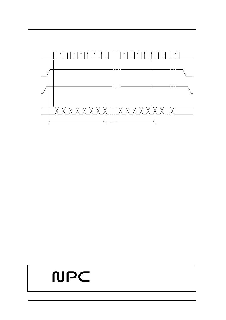
Data Write
Data is input when WR is HIGH and CE is HIGH.
The seconds’ digit signal to the timer counter stops
on the first falling edge of CLK and the counter
remains stopped until the next rising edge of CE. The
1 Hz to 128 Hz frequency divider step counters are
reset during the interval between the first and second
rising edges of CLK.
The data is then input on DATA into the shift regis-
ter, starting with seconds’ digit LSB synchronized
with the rising edge of CLK.
After the final data is input into the shift register fol-
lowing 52 cycles, the shift register contents are trans-
WR
CE
CLK
DATA
S1
second
year
FDT
S40
S20
S10
S8
S4
S2
y80
y40
y20
y10
y8
1
2
3
52
53
54
54+n
INPUT MODE
ferred to the timer counters. Note that a data write
must contain 52 bits of input data. If CE goes LOW
before 52 bits are input, the input data is invalid. If
the input data exceeds 52 bits, data from the 53rd bit
is ignored (the first 52 bits remain valid).
The data write time should be completed after
t
CE
≤
0.9 s.
If a data read occurs immediately after a data write, a
wait time (t
RCV
) is required if CE has gone LOW.
Note that writing null data will cause incorrect oper-
ation. All bits must be valid data bits.
相關PDF資料 |
PDF描述 |
|---|---|
| NR8576AB | Real-time Clock Modules |
| NS8AT | Glass Passivated General Purpose Plastic Rectifier(鈍化玻璃通用塑膠整流器) |
| NS8BT | Glass Passivated General Purpose Plastic Rectifier(鈍化玻璃通用塑膠整流器) |
| NSB8AT | Glass Passivated General Purpose Plastic Rectifier(鈍化玻璃通用塑膠整流器) |
| NSB8MT | Glass Passivated General Purpose Plastic Rectifier(鈍化玻璃通用塑膠整流器) |
相關代理商/技術參數 |
參數描述 |
|---|---|
| NR8576AB | 制造商:NPC 制造商全稱:Nippon Precision Circuits Inc 功能描述:Real-time Clock Modules |
| NR8576BA | 制造商:NPC 制造商全稱:Nippon Precision Circuits Inc 功能描述:Real-time Clock Modules |
| NR8576BB | 制造商:NPC 制造商全稱:Nippon Precision Circuits Inc 功能描述:Real-time Clock Modules |
| NR8576SERIES | 制造商:未知廠家 制造商全稱:未知廠家 功能描述:Real-time Clock Modules |
| NR8800FS-CB | 制造商:RENESAS 制造商全稱:Renesas Technology Corp 功能描述:φ 80 μm InGaAs AVALANCHE PHOTO DIODE MODULE FOR OTDR APPLICATIONS |
發布緊急采購,3分鐘左右您將得到回復。