- 您現(xiàn)在的位置:買賣IC網(wǎng) > PDF目錄361167 > NUS5530MN (ON SEMICONDUCTOR) Integrated Power MOSFET with PNP Low VCE(sat) Switching Transistor PDF資料下載
參數(shù)資料
| 型號: | NUS5530MN |
| 廠商: | ON SEMICONDUCTOR |
| 英文描述: | Integrated Power MOSFET with PNP Low VCE(sat) Switching Transistor |
| 中文描述: | 集成功率MOSFET與進(jìn)步黨低Vce(sat)開關(guān)晶體管 |
| 文件頁數(shù): | 1/9頁 |
| 文件大?。?/td> | 167K |
| 代理商: | NUS5530MN |
Semiconductor Components Industries, LLC, 2006
May, 2006
Rev. 0
1
Publication Order Number:
NUS5530MN/D
NUS5530MN
Integrated Power MOSFET
with PNP Low V
CE(sat)
Switching Transistor
This integrated device represents a new level of safety and
board
space reduction by combining the 20 V P
Channel FET with a
PNP Silicon Low V
CE(sat)
switching transistor. This newly integrated
product provides higher efficiency and accuracy for battery powered
portable electronics.
Features
Low R
DS(on)
(MOSFET) and Low V
CE(sat)
(Transistor)
Higher Efficiency Extending Battery Life
Logic Level Gate Drive (MOSFET)
Performance DFN Package
This is a Pb
Free Device
Applications
Power Management in Portable and Battery
Powered Products; i.e.,
Cellular and Cordless Telephones and PCMCIA Cards
MAXIMUM RATINGS FOR P
CHANNEL FET
(T
A
= 25
°
C unless otherwise noted)
Rating
Symbol
5 sec
Steady
State
Unit
Drain
Source Voltage
V
DS
20
V
Gate
Source Voltage
V
GS
12
V
Continuous Drain Current
(T
J
= 150
°
C) (Note 1)
T
A
= 25
°
C
T
A
= 85
°
C
I
D
5.3
3.8
3.9
2.8
A
Pulsed Drain Current
I
DM
20
A
Continuous Source Current
(Note 1)
I
S
5.3
3.9
A
Maximum Power Dissipation
(Note 1)
T
A
= 25
°
C
T
A
= 85
°
C
P
D
2.5
1.3
1.3
0.7
W
Operating Junction and Storage
Temperature Range
T
J
, T
stg
55 to +150
°
C
Stresses exceeding Maximum Ratings may damage the device. Maximum
Ratings are stress ratings only. Functional operation above the Recommended
Operating Conditions is not implied. Extended exposure to stresses above the
Recommended Operating Conditions may affect device reliability.
1. Surface Mounted on FR4 Board using 1 in sq pad size
(Cu area = 1.27 in sq [1 oz] including traces).
Device
Package
Shipping
ORDERING INFORMATION
http://onsemi.com
For information on tape and reel specifications,
including part orientation and tape sizes, please
refer to our Tape and Reel Packaging Specifications
Brochure, BRD8011/D.
NUS5530MNR2G
DFN8
(Pb
Free)
3000/Tape & Reel
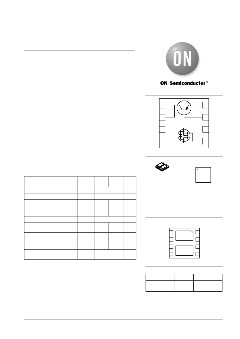
DFN8
CASE 506AL
N/C
Collector
Source
Drain
Emitter
Base
N/C
Gate
(Bottom View)
PIN ASSIGNMENT
A
Y
WW
= Assembly Location
= Year
= Work Week
= Pb
Free Package
1
2
3
4
8
7
6
5
1
8
Collector
Drain
(Top View)
1
2
3
4
8
7
6
5
1
MARKING DIAGRAM
5530
AYWW
(Note: Microdot may be in either location)
相關(guān)PDF資料 |
PDF描述 |
|---|---|
| NVC1001 | 4 Ch Color Video Display ASIC Solution for Multiplexer |
| NX26F011A | 4 Mbit Uniform Sector, Serial Flash Memory |
| NX26F011A-3V-R | 4 Mbit Uniform Sector, Serial Flash Memory |
| NX26F011A-5V-R | 4 Mbit Uniform Sector, Serial Flash Memory |
| NX26F041A | 4 Mbit Uniform Sector, Serial Flash Memory |
相關(guān)代理商/技術(shù)參數(shù) |
參數(shù)描述 |
|---|---|
| NUS5530MNR2G | 功能描述:MOSFET INTEGRATED POWER BJT RoHS:否 制造商:STMicroelectronics 晶體管極性:N-Channel 汲極/源極擊穿電壓:650 V 閘/源擊穿電壓:25 V 漏極連續(xù)電流:130 A 電阻汲極/源極 RDS(導(dǎo)通):0.014 Ohms 配置:Single 最大工作溫度: 安裝風(fēng)格:Through Hole 封裝 / 箱體:Max247 封裝:Tube |
| NUS5531MT | 制造商:ONSEMI 制造商全稱:ON Semiconductor 功能描述:Main Switch Power MOSFET and Single Charging BJT |
| NUS5531MTR2G | 功能描述:MOSFET 12V PFET W 20V PNP RoHS:否 制造商:STMicroelectronics 晶體管極性:N-Channel 汲極/源極擊穿電壓:650 V 閘/源擊穿電壓:25 V 漏極連續(xù)電流:130 A 電阻汲極/源極 RDS(導(dǎo)通):0.014 Ohms 配置:Single 最大工作溫度: 安裝風(fēng)格:Through Hole 封裝 / 箱體:Max247 封裝:Tube |
| NUS6160MN | 制造商:ONSEMI 制造商全稱:ON Semiconductor 功能描述:Low Profile Overvoltage Protection IC with Integrated MOSFET |
| NUS6160MNTWG | 功能描述:MOSFET OVP IC W/INTEGRTD MO RoHS:否 制造商:STMicroelectronics 晶體管極性:N-Channel 汲極/源極擊穿電壓:650 V 閘/源擊穿電壓:25 V 漏極連續(xù)電流:130 A 電阻汲極/源極 RDS(導(dǎo)通):0.014 Ohms 配置:Single 最大工作溫度: 安裝風(fēng)格:Through Hole 封裝 / 箱體:Max247 封裝:Tube |
發(fā)布緊急采購,3分鐘左右您將得到回復(fù)。