- 您現在的位置:買賣IC網 > PDF目錄382378 > PCA9532 (NXP Semiconductors N.V.) 16-bit I2C LED dimmer PDF資料下載
參數資料
| 型號: | PCA9532 |
| 廠商: | NXP Semiconductors N.V. |
| 英文描述: | 16-bit I2C LED dimmer |
| 中文描述: | 16位I2C LED調光 |
| 文件頁數: | 12/20頁 |
| 文件大小: | 154K |
| 代理商: | PCA9532 |
Philips Semiconductors
Product data
PCA9532
16-bit I
2
C LED dimmer
2003 May 02
12
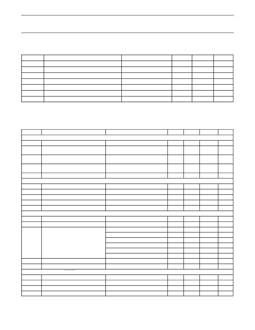
ABSOLUTE MAXIMUM RATINGS
In accordance with the Absolute Maximum Rating System (IEC 134)
SYMBOL
PARAMETER
CONDITIONS
MIN
MAX
UNIT
V
DD
V
I/O
I
I/O
I
SS
P
tot
T
stg
T
amb
Supply voltage
-0.5
6.0
V
DC voltage on an I/O
V
SS
- 0.5
—
5.5
V
DC output current on an I/O
±
25
mA
Supply current
—
200
mA
Total power dissipation
—
400
mW
Storage temperature range
-65
+150
°
C
°
C
Operating ambient temperature
-40
+85
HANDLING
Inputs and outputs are protected against electrostatic discharge in normal handling. However, to be totally safe, it is desirable to take
precautions appropriate to handling MOS devices. Advice can be found in Data Handbook IC24 under
”
Handling MOS devices
”
.
DC CHARACTERISTICS
V
DD
= 2.3 to 5.5 V; V
SS
= 0 V; T
amb
= -40 to +85
°
C; unless otherwise specified. TYP at 3.3 V and 25
°
C.
SYMBOL
PARAMETER
Supplies
V
DD
Supply voltage
CONDITIONS
MIN
TYP
MAX
UNIT
2.3
—
5.5
V
I
DD
Supply current
Operating mode; V
DD
= 5.5 V; no load;
V
I
= V
DD
or V
SS
; f
SCL
= 100 kHz
Standby mode; V
DD
= 5.5 V; no load;
V
I
= V
DD
or V
SS
; f
SCL
= 0 kHz
Standby mode; V
DD
= 5.5 V; Every
LED I/O at V
IN
= 4.3 V; f
SCL
= 0 kHz
V
DD
= 3.3 V; no load; V
I
= V
DD
or V
SS
—
350
550
μ
A
I
stb
Standby current
—
2.1
5.0
μ
A
I
DD
Additional standby current
—
—
2
mA
V
POR
Power-on reset voltage
—
1.7
2.2
V
Input SCL; input/output SDA
V
IL
LOW-level input voltage
V
IH
HIGH-level input voltage
I
OL
LOW-level output current
I
L
Leakage current
C
I
Input capacitance
I/Os
V
IL
LOW-level input voltage
V
IH
HIGH-level input voltage
-0.5
0.7 V
DD
3
-1
—
—
—
6.5
—
4.4
0.3 V
DD
5.5
—
+1
5
V
V
V
OL
= 0.4V
V
I
= V
DD
= V
SS
V
I
= V
SS
mA
μ
A
pF
-0.5
2.0
9
12
15
15
20
25
-1
—
—
—
—
—
—
—
—
—
—
2.6
0.8
5.5
—
—
—
—
—
—
1
5
V
V
V
OL
= 0.4 V; V
DD
= 2.3 V; Note 1
V
OL
= 0.4 V; V
DD
= 3.0 V; Note 1
V
OL
= 0.4 V; V
DD
= 5.0 V; Note 1
V
OL
= 0.7 V; V
DD
= 2.3 V; Note 1
V
OL
= 0.7 V; V
DD
= 3.0 V; Note 1
V
OL
= 0.7 V; V
DD
= 5.0 V; Note 1
V
DD
= 3.6 V; V
I
= 0 or V
DD
mA
mA
mA
mA
mA
mA
μ
A
pF
I
OL
LOW-level output current
I
L
Input leakage current
Input/output capacitance
C
IO
Select Inputs A0, A1, A2 / RESET
V
IL
LOW-level input voltage
V
IH
HIGH-level input voltage
I
LI
Input leakage current
C
I
Input capacitance
NOTE:
1. Each I/O must be externally limited to a maximum of 25 mA and each octal (LED0-LED7 and LED8-LED15) must be limited to a maximum
current of 100 mA for a device total of 200 mA.
-0.5
2.0
-1
—
—
—
—
2.3
0.8
5.5
1
5
V
V
μ
A
pF
V
I
= V
SS
相關PDF資料 |
PDF描述 |
|---|---|
| PCA9533 | 4-bit I2C LED dimmer |
| PCA9533D01 | 4-bit I2C LED dimmer |
| PCA9533D02 | 4-bit I2C LED dimmer |
| PCA9533DP01 | 4-bit I2C LED dimmer |
| PCA9533DP02 | 4-bit I2C LED dimmer |
相關代理商/技術參數 |
參數描述 |
|---|---|
| PCA9532BS | 制造商:PHILIPS 制造商全稱:NXP Semiconductors 功能描述:16-bit I2C-bus LED dimmer |
| PCA9532BS,118 | 功能描述:LED照明驅動器 I2C LED DIMMER 16BIT RoHS:否 制造商:STMicroelectronics 輸入電壓:11.5 V to 23 V 工作頻率: 最大電源電流:1.7 mA 輸出電流: 最大工作溫度: 安裝風格:SMD/SMT 封裝 / 箱體:SO-16N |
| PCA9532BS-T | 功能描述:LED照明驅動器 I2C LED DIMMER 16BIT RoHS:否 制造商:STMicroelectronics 輸入電壓:11.5 V to 23 V 工作頻率: 最大電源電流:1.7 mA 輸出電流: 最大工作溫度: 安裝風格:SMD/SMT 封裝 / 箱體:SO-16N |
| PCA9532D | 功能描述:LED照明驅動器 I2C LED DIMMER 16BIT RoHS:否 制造商:STMicroelectronics 輸入電壓:11.5 V to 23 V 工作頻率: 最大電源電流:1.7 mA 輸出電流: 最大工作溫度: 安裝風格:SMD/SMT 封裝 / 箱體:SO-16N |
| PCA9532D,112 | 功能描述:LED照明驅動器 I2C LED DIMMER 16BIT RoHS:否 制造商:STMicroelectronics 輸入電壓:11.5 V to 23 V 工作頻率: 最大電源電流:1.7 mA 輸出電流: 最大工作溫度: 安裝風格:SMD/SMT 封裝 / 箱體:SO-16N |
發布緊急采購,3分鐘左右您將得到回復。