- 您現在的位置:買賣IC網 > PDF目錄382379 > PCA9559PWDH (NXP SEMICONDUCTORS) 5-bit multiplexed/1-bit latched 6-bit I2C EEPROM PDF資料下載
參數資料
| 型號: | PCA9559PWDH |
| 廠商: | NXP SEMICONDUCTORS |
| 元件分類: | 通用總線功能 |
| 英文描述: | 5-bit multiplexed/1-bit latched 6-bit I2C EEPROM |
| 中文描述: | 2 LINE TO 1 LINE MULTIPLEXER, TRUE OUTPUT, PDSO20 |
| 封裝: | TSSOP-20 |
| 文件頁數: | 3/11頁 |
| 文件大小: | 83K |
| 代理商: | PCA9559PWDH |
Philips Semiconductors
Product data
PCA9559
5-bit multiplexed/1-bit latched 6-bit
I
2
C EEPROM DIP switch
2003 Jun 27
3
FUNCTIONAL DESCRIPTION
When the MUX_SELECT signal is logic 0, the multiplexer will select
the data from the non-volatile register to drive on the MUX_OUT
pins. When the MUX_SELECT signal is logic 1, the multiplexer will
select the MUX_IN lines to drive on the MUX_OUT pins. The
MUX_SELECT signal is also used to latch the NON_MUXED_OUT
signal which outputs data from the non-volatile register. The
NON_MUXED_OUT signal latch is transparent when MUX_SELECT
is in a logic 0 state, and will latch data when MUX_SELECT is in a
logic 1 state. When the active-LOW OVERRIDE_N signal is set to
logic 0 and the MUX_SELECT signal is at a logic 0, all outputs will
be driven to logic 0. This information is summarized in Table 1.
The Write Protect (WP) input is used to control the ability to write the
contents of the 6-bit non-volatile register. If the WP signal is logic 0,
the I
2
C-bus will be able to write the contents of the non-volatile
register. If the WP signal is logic 1, data will not be allowed to be
written into the non-volatile register.
The factory default for the contents of the non-volatile register are all
logic 0. These stored values can be read or written using the
I
2
C-bus (described in the next section).
The OVERRIDE_N, WP, MUX_IN, and MUX_SELECT signals have
internal pull-up resistors. See the DC and AC Characteristics for
hysteresis and signal spike suppression figures.
FUNCTION TABLE
OVERRIDE_N
MUX_SELECT
MUX_OUT
OUTPUTS
NON_MUXED_OUT
OUTPUT
0
0
All 0
’
s
All 0
’
s
0
1
MUX_IN
inputs
Latched
NON_MUXED
_OUT
1
1
0
From non-
volatile
register
From non-volatile
register
1
1
MUX_IN
inputs
From non-volatile
register
NOTE:
1. NON_MUXED_OUT state will be the value present on the output
at the time of the MUX_SELECT input transitioned from a logic 0
to a logic 1 state.
I
2
C INTERFACE
Communicating with this device is initiated by sending a valid
address on the I
2
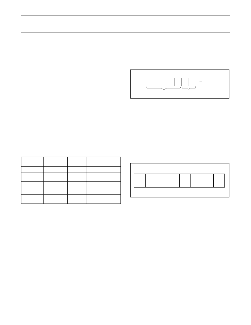
C-bus. The address format (see FIgure 1) has 5
fixed bits and two user-programmable bits followed by a 1-bit
read/write value which determines the direction of the data transfer.
1
0
0
1
A1
A0
FIXED
HARDWARE
SELECTABLE
R/W
1
LSB
MSB
Figure 2. I
2
C Address Byte
Following the address and acknowledge bit are 8 data bits which,
depending on the read/write bit in the address, will read data from or
write data to the non-volatile register. Data will be written to the
register if the read/write bit is logic 0 and the WP input is logic 0.
Data will be read from the register if the bit is logic 1. The four
high-order bits are latched outputs, while the four low order bits are
multiplexed outputs (Figure 3).
NOTE:
1. To ensure data integrity, the non-volatile register must be
internally write protected when V
CC
to the I
2
C-bus is powered
down or V
CC
to the component is dropped below normal
operating levels.
LSB
MSB
MUX
DATA A
MUX
DATA B
MUX
DATA C
MUX
DATA D
NON-
MUXED
DATA
0
0
MUX
DATA E
Figure 3. I
2
C Data Byte
POWER-ON RESET (POR)
When power is applied to V
CC
, an internal power-on reset holds the
PCA9559 in a reset state until V
CC
has reached V
POR
. At that point,
the reset condition is released and the PCA9559 volatile registers
and I
2
C/SMBus state machine will initialize to their default states.
The MUX_OUT and NON_MUXED_OUT pin values depend on:
-
the OVERRIDE # and MUX_SELECT logic levels
-
the previously stored values in the EEPROM register/current
MUX_IN pin values as shown in the Function Table.
相關PDF資料 |
PDF描述 |
|---|---|
| PCA9560 | The CAT24FC02 is a 2-kb Serial CMOS EEPROM internally organized as 256 words of 8 bits each |
| PCA9560D | The CAT24FC02 is a 2-kb Serial CMOS EEPROM internally organized as 256 words of 8 bits each |
| PCB2032V | EEPROM |
| PCB2320DP | ISDN Line Interface |
| PCB2325DP | ISDN Line Interface |
相關代理商/技術參數 |
參數描述 |
|---|---|
| PCA9560D | 功能描述:電可擦除可編程只讀存儲器 DUAL5BTMUX 1B LATCH I2C EPROM RoHS:否 制造商:Atmel 存儲容量:2 Kbit 組織:256 B x 8 數據保留:100 yr 最大時鐘頻率:1000 KHz 最大工作電流:6 uA 工作電源電壓:1.7 V to 5.5 V 最大工作溫度:+ 85 C 安裝風格:SMD/SMT 封裝 / 箱體:SOIC-8 |
| PCA9560D,112 | 功能描述:多路器開關 IC DUAL5BTMUX 1B LATCH RoHS:否 制造商:Texas Instruments 通道數量:1 開關數量:4 開啟電阻(最大值):7 Ohms 開啟時間(最大值): 關閉時間(最大值): 傳播延遲時間:0.25 ns 工作電源電壓:2.3 V to 3.6 V 工作電源電流: 最大工作溫度:+ 85 C 安裝風格:SMD/SMT 封裝 / 箱體:UQFN-16 |
| PCA9560D,118 | 功能描述:多路器開關 IC DUAL5BTMUX 1B LATCH RoHS:否 制造商:Texas Instruments 通道數量:1 開關數量:4 開啟電阻(最大值):7 Ohms 開啟時間(最大值): 關閉時間(最大值): 傳播延遲時間:0.25 ns 工作電源電壓:2.3 V to 3.6 V 工作電源電流: 最大工作溫度:+ 85 C 安裝風格:SMD/SMT 封裝 / 箱體:UQFN-16 |
| PCA9560D-T | 功能描述:電可擦除可編程只讀存儲器 DUAL5BTMUX 1B LATCH I2C EPROM RoHS:否 制造商:Atmel 存儲容量:2 Kbit 組織:256 B x 8 數據保留:100 yr 最大時鐘頻率:1000 KHz 最大工作電流:6 uA 工作電源電壓:1.7 V to 5.5 V 最大工作溫度:+ 85 C 安裝風格:SMD/SMT 封裝 / 箱體:SOIC-8 |
| PCA9560PW | 功能描述:電可擦除可編程只讀存儲器 DUAL5BTMUX 1B LATCH I2C EPROM RoHS:否 制造商:Atmel 存儲容量:2 Kbit 組織:256 B x 8 數據保留:100 yr 最大時鐘頻率:1000 KHz 最大工作電流:6 uA 工作電源電壓:1.7 V to 5.5 V 最大工作溫度:+ 85 C 安裝風格:SMD/SMT 封裝 / 箱體:SOIC-8 |
發(fā)布緊急采購,3分鐘左右您將得到回復。