- 您現在的位置:買賣IC網 > PDF目錄382380 > PCD5032 (NXP SEMICONDUCTORS) ADPCM CODEC for digital cordless telephones PDF資料下載
參數資料
| 型號: | PCD5032 |
| 廠商: | NXP SEMICONDUCTORS |
| 元件分類: | 編解碼器 |
| 英文描述: | ADPCM CODEC for digital cordless telephones |
| 中文描述: | A-LAW, ADPCM CODEC, PQFP44 |
| 封裝: | 14 X 14 MM, PLASTIC, SOT-205AG, QFP-44 |
| 文件頁數: | 15/24頁 |
| 文件大小: | 136K |
| 代理商: | PCD5032 |
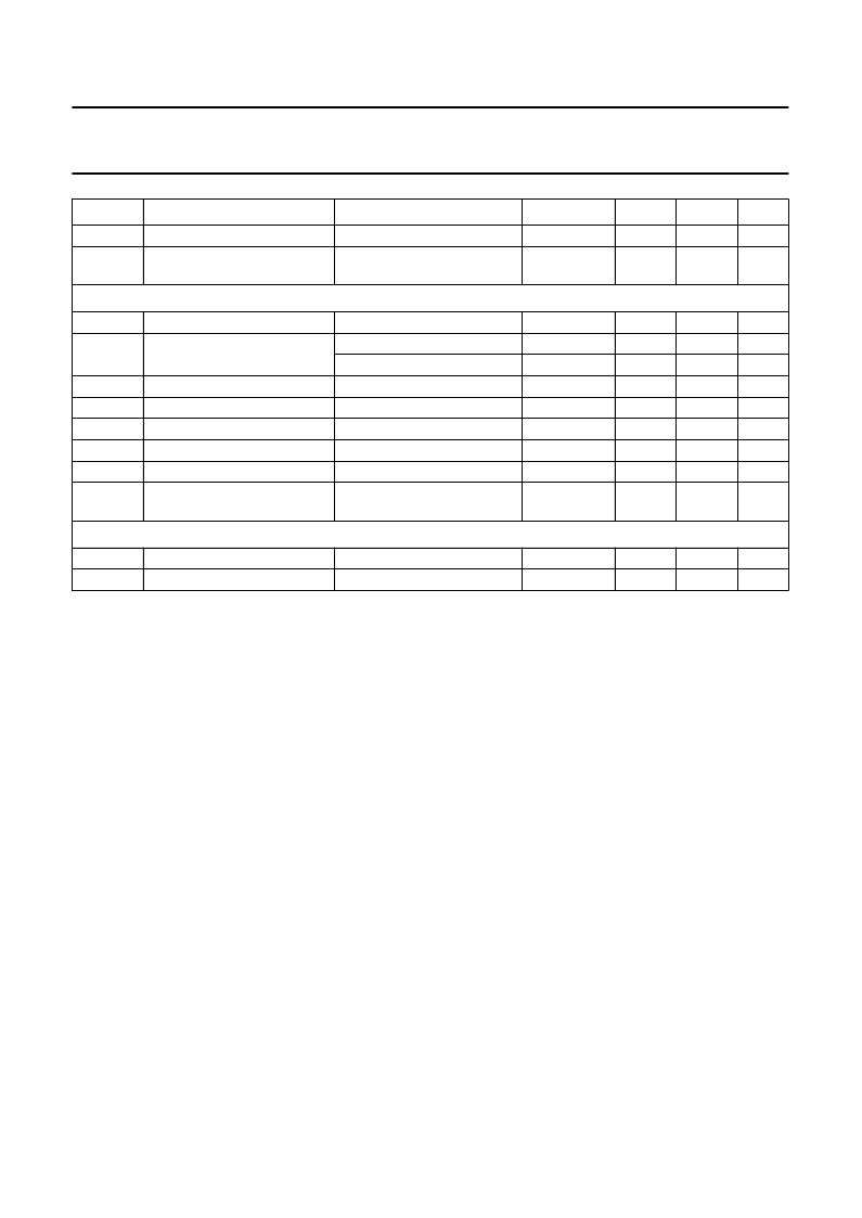
1997 Apr 03
15
Philips Semiconductors
Product specification
ADPCM CODEC for digital cordless
telephones
PCD5032
Notes
1.
All outputs left open. I
DD
measured with all inputs connected to V
SS
, except: CLK and DCLK connected to 3.456 MHz;
RAS and TAS connected to 8 kHz. I
stb
measured with all inputs connected to V
SS
, except: TM+, TM
left open.
The reference voltage is available on V
REF+
and V
REF
and is measured with respect to VGA. The voltage outputs
are intended for electret microphone supply and can deliver 400
μ
A.
Digital inputs and outputs are CMOS-levels compatible. The outputs and inputs can sink or source 1 mA. Pull-down
resistors are present at pins RPI, TPI, TEST, RAD.
Any frequency between min. and max. is allowed for DCLK. The signals CLK and RAS/TAS must be
frequency-locked and will have a ratio of f
CLK
/f
RAS
= 432
All analog input/output voltages are measured differentially. The circuit is designed for use with an electret
microphone.
Frequency band is 300 Hz to 3400 Hz. Maximum load capacitance = 100 pF differentially, or 200 pF each pin.
Nominal signal level gives
10 dBm0 on the PCM interface (G.711/G.712). Value given for TX gain setting 0 dB.
Nominal signal level gives 3.14 dBm0 on the PCM interface, with larger input signals the digital output will be
saturated. Value given for TX gain setting 0 dB.
Transmitter gain setting = 0 dB and input signal level = 40 mV (RMS) (will generate 0 dBm0 on PCM interface
according to G.711).
10. PCM signal level is 0 dBm0 and RX gain setting 0 dB. With a load of 300
between RE+ and RE
the signal level
results in an output power of 1 mW. The maximum output current is 10 mA.
11. PCM signal level is +3.14 dBm0 and RX gain setting +4 dB. The maximum output current is 10 mA.
12. PCM signal level is 0 dBm0 (G.711).
13. For maximum output power the load resistance should equal the typical output impedance (specified at
I
LOAD
20 mA). The absolute maximum value of output power given in Chapter 9 defines the minimum load
resistance.
2.
3.
4.
5.
6.
7.
8.
9.
G
v(step)
THD
TX
voltage gain, step size
total harmonic distortion
(transmitted)
1
40
dB
dB
note 9
Receiver audio output
Z
o
V
o(rms)
output impedance
output signal level (RMS
value)
note 6
0 dBm0; note 10
3.14 dBm0; note 11
4
+3
36
10
550
1250
3
+4
1
6.0
2
+5
0
40
mV
mV
dB
dB
dB
dB
dB
dB
G
v(min)
G
v(max)
G
v(step)
G
vol
G
vol(step)
THD
RX
minimum voltage gain
maximum voltage gain
voltage gain, step size
volume control range
volume step size
total harmonic distortion
(received)
note 12
Ringer output
; notes 5 and 13
Z
o
G
vol
output impedance
volume control range
29
14
29
+4
dB
SYMBOL
PARAMETER
CONDITIONS
MIN.
TYP.
MAX.
UNIT
相關PDF資料 |
PDF描述 |
|---|---|
| PCD5032H | ADPCM CODEC for digital cordless telephones |
| PCD5032T | ADPCM CODEC for digital cordless telephones |
| PCD5041 | DECT burst mode controller |
| PCD5041H | DECT burst mode controller |
| PCD5041HZ | DECT burst mode controller |
相關代理商/技術參數 |
參數描述 |
|---|---|
| PCD5032B | 制造商:未知廠家 制造商全稱:未知廠家 功能描述:Linear CODEC |
| PCD5032D | 制造商:未知廠家 制造商全稱:未知廠家 功能描述:Linear CODEC |
| PCD5032H | 制造商:PHILIPS 制造商全稱:NXP Semiconductors 功能描述:ADPCM CODEC for digital cordless telephones |
| PCD5032T | 制造商:PHILIPS 制造商全稱:NXP Semiconductors 功能描述:ADPCM CODEC for digital cordless telephones |
| PCD5040 | 制造商:未知廠家 制造商全稱:未知廠家 功能描述:DECT |
發布緊急采購,3分鐘左右您將得到回復。