- 您現在的位置:買賣IC網 > PDF目錄382382 > PCK210 Low voltage dual 1:5 differential ECL/PECL clock driver PDF資料下載
參數資料
| 型號: | PCK210 |
| 英文描述: | Low voltage dual 1:5 differential ECL/PECL clock driver |
| 中文描述: | 低電壓雙1:5差動ECL / PECL的時鐘驅動器 |
| 文件頁數: | 2/8頁 |
| 文件大小: | 71K |
| 代理商: | PCK210 |
Philips Semiconductors
Product data
PCK210
Low voltage dual 1:5 differential
ECL/PECL clock driver
2
2002 Dec 13
FEATURES
85 ps part-to-part skew typical
20 ps output-to-output skew typical
Differential design
V
BB
output
Voltage and temperature compensated outputs
Low voltage V
EE
range of -2.25 V to -3.8 V
75 k
input pull-down resistors
Form, fit, and function compatible with MC100EP210
DESCRIPTION
The PCK210 is a low skew 1-to-5 dual differential driver, designed
with clock distribution in mind. The input signals can be either
differential or single-ended if the V
BB
output is used. The signal is
fanned out to 5 identical differential outputs.
The PCK210 is specifically designed, modeled and produced with
low skew as the key goal. Optimal design and layout serve to
minimize gate-to-gate skew within a device, and empirical modeling
is used to determine process control limits that ensure consistent
t
PD
distributions from lot to lot. The net result is a dependable,
guaranteed low skew device.
To ensure that the tight skew specification is met, it is necessary that
both sides of the differential output are terminated into 50
, even if
only one side is being used. In most applications, all ten differential
pairs will be used, and therefore terminated. In the case where fewer
than ten pairs are used, it is necessary to terminate at least the
output pairs on the same package side as the pair(s) being used on
that side, in order to maintain minimum skew. Failure to do this will
result in small degradations of propagation delay (on the order of
10-20 ps) of the output(s) being used, which, while not being
catastrophic to most designs, will mean a loss of skew margin.
The PCK210, as with most other ECL devices, can be operated
from a positive V
CC
supply in PECL mode. This allows the PCK210
to be used for high performance clock distribution in +3.3 V or
+2.5 V systems. Designers can take advantage of the PCK210’s
performance to distribute low skew clocks across the backplane or
the board. In a PECL environment, series or Thevenin line
terminations are typically used as they require no additional power
supplies.
The PCK210 may be driven single-endedly utilizing the V
BB
bias
output with the CLKA or CLKB input. If a single-ended signal is to be
used, the V
BB
pin should be connected to the CLKA or CLKB input
and bypassed to ground via a 0.01
μ
F capacitor. The V
BB
output
can only source/sink 0.3 mA, therefore, it should be used as a
switching reference for the PCK210 only. Part-to-part skew
specifications are not guaranteed when driving the PCK210
single-endedly.
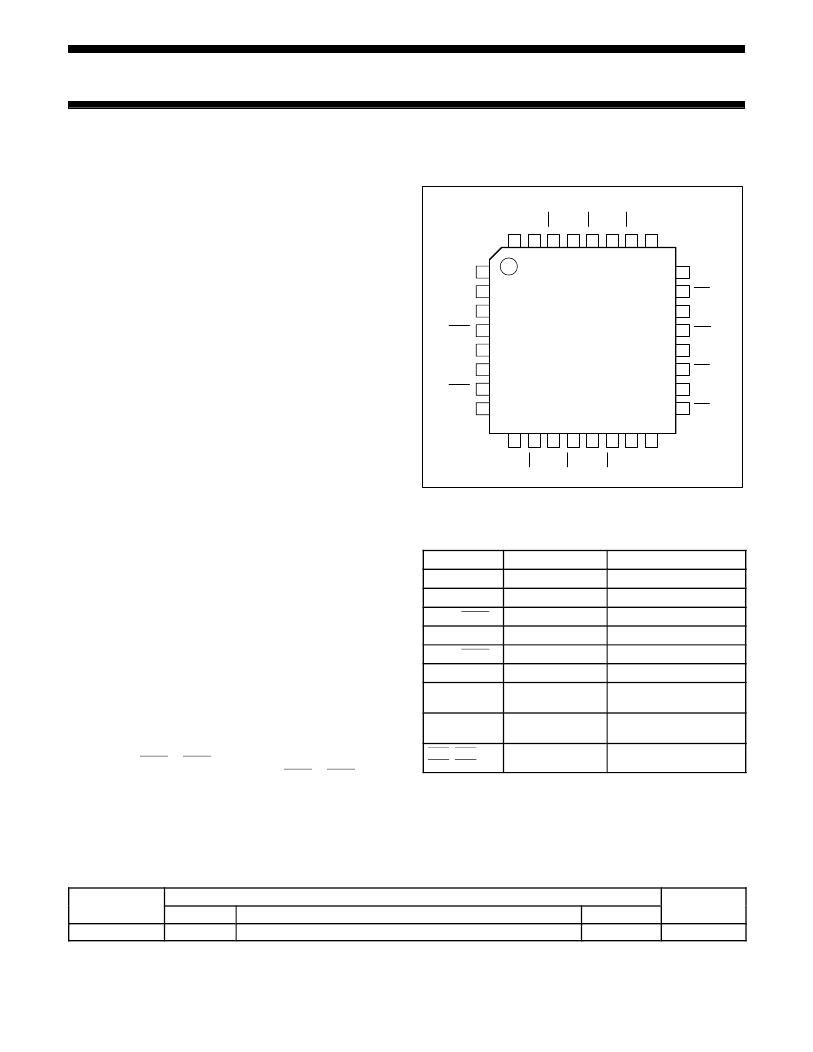
PINNING
Pin configuration
V
BB
24
23
22
21
20
19
18
17
9
1
1
1
1
1
1
1
QA3
QA3
QA4
QA4
QB0
QB0
QB1
QB1
1
2
3
4
5
6
7
8
3
3
3
2
2
2
2
2
PCK210
SW00909
V
Q
Q
Q
Q
Q
Q
NC
CLKA
CLKA
CLKB
CLKB
Q
Q
Q
Q
Q
Q
V
EE
V
CC
C
V
C
V
C
V
C
Figure 1. Pin configuration
Pin description
SYMBOL
PIN
DESCRIPTION
V
CC
NC
1
Supply voltage
2
Not connected
CLKA, CLKA
3, 4
Differential input pair
V
BB
CLKB, CLKB
5
V
BB
output
Differential input pair
6, 7
V
EE
V
CCO
8
Ground
9, 16, 25, 32
Output drive power supply
voltage
QA0-QA4,
QB0-QB4
31, 29, 27, 24, 22,
20, 18, 15, 13, 11
Differential outputs
QA0-QA4 ,
QB0-QB4
30, 28, 26, 23, 21,
19, 17, 14, 12, 10
Differential outputs
ORDERING INFORMATION
Package
Temperature
range
Type number
Name
LQFP32
Description
plastic low profile quad flat package; 32 leads; body 7
×
7
×
1.4 mm
Version
SOT358-1
PCK210BD
-40 to +70
°
C
相關PDF資料 |
PDF描述 |
|---|---|
| PCK2111 | 1:10 LVDS clock distribution device |
| PCK351 | 1:10 clock distribution device with 3-State outputs |
| PCK351D | 1:10 clock distribution device with 3-State outputs |
| PCK3807A | 1:10 LVTTL clock distribution device |
| PCK3807AD | 1:10 LVTTL clock distribution device |
相關代理商/技術參數 |
參數描述 |
|---|---|
| PCK210BD | 制造商:PHILIPS 制造商全稱:NXP Semiconductors 功能描述:Low voltage dual 1-5 differential ECL/PECL clock driver |
| PCK210BD,118 | 功能描述:時鐘緩沖器 DUAL 1:5 ECL/PECL CLOCK DRIVER RoHS:否 制造商:Texas Instruments 輸出端數量:5 最大輸入頻率:40 MHz 傳播延遲(最大值): 電源電壓-最大:3.45 V 電源電壓-最小:2.375 V 最大功率耗散: 最大工作溫度:+ 85 C 最小工作溫度:- 40 C 封裝 / 箱體:LLP-24 封裝:Reel |
| PCK210BD,128 | 功能描述:IC CLK BUFFER 1:5 1.5GHZ 32-LQFP RoHS:是 類別:集成電路 (IC) >> 時鐘/計時 - 時鐘緩沖器,驅動器 系列:- 標準包裝:1 系列:HiPerClockS™ 類型:扇出緩沖器(分配),多路復用器 電路數:1 比率 - 輸入:輸出:2:18 差分 - 輸入:輸出:是/無 輸入:CML,LVCMOS,LVPECL,LVTTL,SSTL 輸出:LVCMOS,LVTTL 頻率 - 最大:250MHz 電源電壓:2.375 V ~ 3.465 V 工作溫度:0°C ~ 70°C 安裝類型:表面貼裝 封裝/外殼:32-LQFP 供應商設備封裝:32-TQFP(7x7) 包裝:- 其它名稱:800-1923-6 |
| PCK210BD,151 | 功能描述:時鐘緩沖器 DUAL 1:5 ECL/PECL CLOCK DRIVER RoHS:否 制造商:Texas Instruments 輸出端數量:5 最大輸入頻率:40 MHz 傳播延遲(最大值): 電源電壓-最大:3.45 V 電源電壓-最小:2.375 V 最大功率耗散: 最大工作溫度:+ 85 C 最小工作溫度:- 40 C 封裝 / 箱體:LLP-24 封裝:Reel |
| PCK210BD,157 | 功能描述:時鐘緩沖器 DUAL 1:5 ECL/PECL CLOCK DRIVER RoHS:否 制造商:Texas Instruments 輸出端數量:5 最大輸入頻率:40 MHz 傳播延遲(最大值): 電源電壓-最大:3.45 V 電源電壓-最小:2.375 V 最大功率耗散: 最大工作溫度:+ 85 C 最小工作溫度:- 40 C 封裝 / 箱體:LLP-24 封裝:Reel |
發布緊急采購,3分鐘左右您將得到回復。