參數資料
| 型號: | PI6C2408-3WE |
| 廠商: | Pericom |
| 文件頁數: | 1/10頁 |
| 文件大小: | 0K |
| 描述: | IC 4+4 0-DELAY CLK BUFF 16-SOIC |
| 產品培訓模塊: | Total Timing Technology |
| 標準包裝: | 48 |
| 類型: | 零延遲緩沖器 |
| PLL: | 帶旁路 |
| 輸入: | TTL |
| 輸出: | TTL |
| 電路數: | 1 |
| 比率 - 輸入:輸出: | 1:8 |
| 差分 - 輸入:輸出: | 無/無 |
| 頻率 - 最大: | 140MHz |
| 除法器/乘法器: | 無/是 |
| 電源電壓: | 3 V ~ 3.6 V |
| 工作溫度: | 0°C ~ 70°C |
| 安裝類型: | 表面貼裝 |
| 封裝/外殼: | 16-SOIC(0.154",3.90mm 寬) |
| 供應商設備封裝: | 16-SOIC |
| 包裝: | 管件 |
1
www.pericom.com
PS8589L
04/30/10
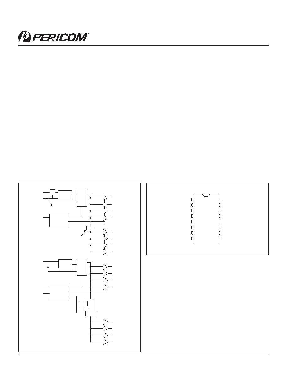
PLL
Option (-3, -4)
CLKIN
FB_IN
SEL1
SEL2
Decode
Logic
Decode
Logic
OUTA1
OUTA2
OUTA3
OUTA4
OUTB2
OUTB3
OUTB4
OUTB1
PI6C2408 (-1, -1H, -2, -3, -4)
÷2
PLL
CLKIN
FB_IN
SEL2
SEL1
OUTA1
OUTA2
OUTA3
OUTA4
OUTB2
OUTB3
OUTB4
OUTB1
PI6C2408-6
MUX
÷2
Option (-2, -3)
MUX
1
2
3
VDD 4
GND 5
OUTA2
6
OUTB2 7
SEL1
8
OUTB1
FB_IN
OUTA3
VDD
OUTB4
OUTB3
SEL2
16
15
14
13
12
11
10
9
CLKIN
OUTA1
GND
OUTA4
16-Pin
W, L
Features
Maximum rated frequency: 140 MHz
Low cycle-to-cycle jitter
Input to output delay, less than 150ps
External feedback pin allows outputs to be synchronized
to the clock input
5V tolerant CLKIN input
Operates at 3.3V VDD
Test mode allows bypass of the PLL for system testing
purposes (e.g., IBIS measurements)
Clock frequency multipliers x to 4x dependent on option
Packaging (Pb-free and Green available):
à
16-pin, 150-mil SOIC (W)
à
16-pin 173-mil TSSOP (L)
Description
The PI6C2408 is a PLL-based, zero-delay buffer, with the ability
to distribute eight outputs of up to 140MHz at 3.3V. Two
banks of four outputs exist, and, depending on product option
ordered, can supply either reference frequency, prescaled half
frequency, or multiplied 2x or 4x input clock frequencies. The
PI6C2408 family has a power-sparing feature: when input SEL2
is 0, the component will 3-state one or both banks of outputs
depending on the state of input SEL1. A PLL bypass test mode
also exists. This product line is available in high-drive and
industrial environment versions.
An external feedback pin is used to synchronize the outputs to
the input; the relationship between loading of this signal and the
other outputs determines the input-output delay.
The PI6C2408 is characterized for both commercial and indus-
trial operation.
Block Diagram
Pin Configuration
PI6C2408
3.3V 4+4 Ouptut Zero-delay Clock Driver
11-0005
相關PDF資料 |
PDF描述 |
|---|---|
| PI6C2408-2WE | IC 4+4 0-DELAY CLK BUFF 16-SOIC |
| VI-J4K-MZ-F1 | CONVERTER MOD DC/DC 40V 25W |
| VI-J4J-MZ-F4 | CONVERTER MOD DC/DC 36V 25W |
| VI-JV2-MZ-F4 | CONVERTER MOD DC/DC 15V 25W |
| MS3452LS22-2PY | CONN RCPT 3POS BOX MNT W/PINS |
相關代理商/技術參數 |
參數描述 |
|---|---|
| PI6C2408-3WEX | 功能描述:鎖相環 - PLL 4+4 Zero Delay Clock Buffer RoHS:否 制造商:Silicon Labs 類型:PLL Clock Multiplier 電路數量:1 最大輸入頻率:710 MHz 最小輸入頻率:0.002 MHz 輸出頻率范圍:0.002 MHz to 808 MHz 電源電壓-最大:3.63 V 電源電壓-最小:1.71 V 最大工作溫度:+ 85 C 最小工作溫度:- 40 C 封裝 / 箱體:QFN-36 封裝:Tray |
| PI6C2408-3WI | 制造商:未知廠家 制造商全稱:未知廠家 功能描述:EIGHT DISTRIBUTED-OUTPUT CLOCK DRIVER|CMOS|SOP|16PIN|PLASTIC |
| PI6C2408-4 | 制造商:未知廠家 制造商全稱:未知廠家 功能描述:Clock IC | 4+4 Output Zero-Delay Clock Driver(Bank A=2XRef. Bank B=2XRef). 10 to 134 MHz |
| PI6C2408-4I | 制造商:未知廠家 制造商全稱:未知廠家 功能描述:Clock IC | 4+4 Output Zero-Delay Clock Driver (Bank A=2XRef. Bank B=2XRef). 10 to 134 MHz. Industrial Temp. Operation |
| PI6C2408-4L | 制造商:PERICOM 制造商全稱:Pericom Semiconductor Corporation 功能描述:Zero-Delay Clock Buffer |
發布緊急采購,3分鐘左右您將得到回復。