- 您現(xiàn)在的位置:買賣IC網(wǎng) > PDF目錄367963 > PI6C2409-1I (Pericom Semiconductor Corp.) Low Input Voltage Current Mode Step-Down DC/DC Controller; Package: SO; No of Pins: 8; Temperature Range: 0°C to +70°C PDF資料下載
參數(shù)資料
| 型號(hào): | PI6C2409-1I |
| 廠商: | Pericom Semiconductor Corp. |
| 英文描述: | Low Input Voltage Current Mode Step-Down DC/DC Controller; Package: SO; No of Pins: 8; Temperature Range: 0°C to +70°C |
| 中文描述: | 時(shí)鐘IC | 9輸出零延遲時(shí)鐘驅(qū)動(dòng)器。工業(yè)溫度。操作 |
| 文件頁數(shù): | 1/8頁 |
| 文件大小: | 167K |
| 代理商: | PI6C2409-1I |
1
PS8613A 07/15/03
1
2
3
4
5
6
7
8
VDD
GND
OUTA2
OUTB2
SEL2
SEL1
OUTB1
OUT0
OUTA4
OUTA3
VDD
GND
OUTB4
OUTB3
16
15
14
13
12
11
10
9
CLKIN
OUTA1
Product Features
Maximum rated frequency: 133 MHz
Low cycle-to-cycle jitter
Input to output delay, less than 200ps
Internal feedback allows outputs to be synchronized
to the clock input
Operates at 3.3V V
DD
Space-saving Packages:
150-mil SOIC (W)
173-mil TSSOP (L)
Functional Description
The PI6C2409 is a PLL based, zero-delay buffer, with the ability
to distribute nine outputs of up to 133MHz at 3.3V.
All the outputs are distributed from a single clock input CLKIN and
output OUT0 performs zero delay by connecting a feedback to PLL.
PI6C2409 has two banks of four outputs that can be controlled by
the selection inputs, SEL1 & SEL2. It also has a powersparing feature:
when input SEL1 is 0 and SEL2 is 1, PLL is turned off and all
outputs are referenced from CLKIN. PI6C2409 is available in
high drive and industrial environment versions.
An internal feedback on OUT0 is used to synchronize the
outputs to the input; the relationship between loading of this signal
and the outputs determines the input-output delay.
PI6C2409 are characterized for both commercial and
industrial operation
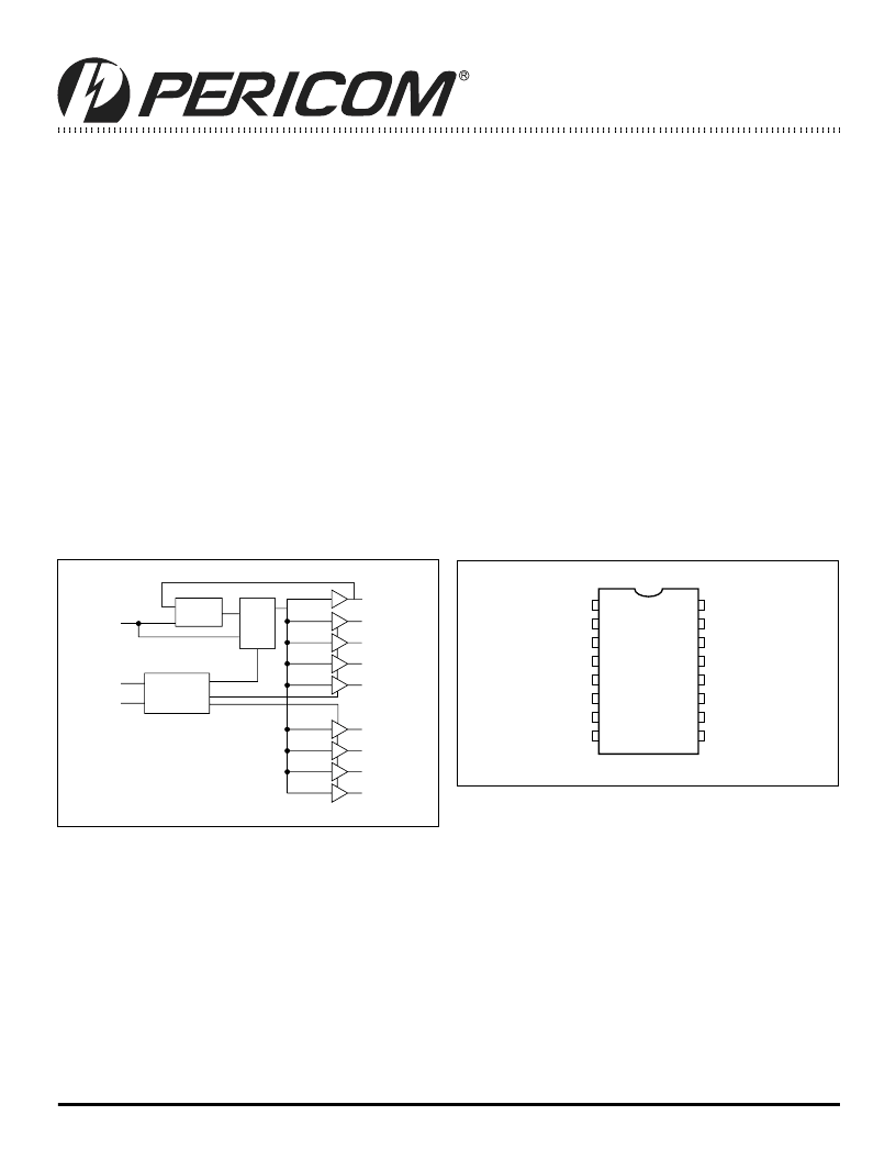
Block Diagram
Pin Configuration
12345678901234567890123456789012123456789012345678901234567890121234567890123456789012345678901212345678901234567890123456789012123456789012
12345678901234567890123456789012123456789012345678901234567890121234567890123456789012345678901212345678901234567890123456789012123456789012
16-Pin
W, L
PLL
CLKIN
SEL1
SEL2
Decode
Logic
OUTA1
OUTA2
OUTA3
OUTA4
OUTB2
OUTB3
OUTB4
OUTB1
PI6C2409(-1, -1H)
MUX
OUT0
相關(guān)PDF資料 |
PDF描述 |
|---|---|
| PI6C2410 | PCI-X Clock Buffers |
| PI6C2410LE | PCI-X Clock Buffers |
| PI6C2410QE | PCI-X Clock Buffers |
| PI6C2410L | PCI-X Clock Buffers |
| PI6C2410Q | PCI-X Clock Buffers |
相關(guān)代理商/技術(shù)參數(shù) |
參數(shù)描述 |
|---|---|
| PI6C2409-1LIE | 功能描述:鎖相環(huán) - PLL 4+4+1 Zero Delay Clock Buffer RoHS:否 制造商:Silicon Labs 類型:PLL Clock Multiplier 電路數(shù)量:1 最大輸入頻率:710 MHz 最小輸入頻率:0.002 MHz 輸出頻率范圍:0.002 MHz to 808 MHz 電源電壓-最大:3.63 V 電源電壓-最小:1.71 V 最大工作溫度:+ 85 C 最小工作溫度:- 40 C 封裝 / 箱體:QFN-36 封裝:Tray |
| PI6C2409-1LIEX | 功能描述:鎖相環(huán) - PLL 4+4+1 Zero Delay Clock Buffer RoHS:否 制造商:Silicon Labs 類型:PLL Clock Multiplier 電路數(shù)量:1 最大輸入頻率:710 MHz 最小輸入頻率:0.002 MHz 輸出頻率范圍:0.002 MHz to 808 MHz 電源電壓-最大:3.63 V 電源電壓-最小:1.71 V 最大工作溫度:+ 85 C 最小工作溫度:- 40 C 封裝 / 箱體:QFN-36 封裝:Tray |
| PI6C2409-1LX | 制造商:Pericom Semiconductor Corporation 功能描述:5V OCTAL 10-BIT BUFFER |
| PI6C2409-1W | 制造商:PERICOM 制造商全稱:Pericom Semiconductor Corporation 功能描述:Zero-Delay Clock Buffer |
| PI6C2409-1WE | 功能描述:鎖相環(huán) - PLL 4+4+1 Zero Delay Clock Buffer RoHS:否 制造商:Silicon Labs 類型:PLL Clock Multiplier 電路數(shù)量:1 最大輸入頻率:710 MHz 最小輸入頻率:0.002 MHz 輸出頻率范圍:0.002 MHz to 808 MHz 電源電壓-最大:3.63 V 電源電壓-最小:1.71 V 最大工作溫度:+ 85 C 最小工作溫度:- 40 C 封裝 / 箱體:QFN-36 封裝:Tray |
發(fā)布緊急采購,3分鐘左右您將得到回復(fù)。