- 您現(xiàn)在的位置:買賣IC網(wǎng) > PDF目錄69049 > PKD01BIFP (ANALOG DEVICES INC) SPECIALTY ANALOG CIRCUIT, PDIP14 PDF資料下載
參數(shù)資料
| 型號: | PKD01BIFP |
| 廠商: | ANALOG DEVICES INC |
| 元件分類: | 模擬信號調(diào)理 |
| 英文描述: | SPECIALTY ANALOG CIRCUIT, PDIP14 |
| 封裝: | PLASTIC, DIP-14 |
| 文件頁數(shù): | 1/18頁 |
| 文件大小: | 402K |
| 代理商: | PKD01BIFP |
REV. A
Information furnished by Analog Devices is believed to be accurate and
reliable. However, no responsibility is assumed by Analog Devices for its
use, nor for any infringements of patents or other rights of third parties
which may result from its use. No license is granted by implication or
otherwise under any patent or patent rights of Analog Devices.
a
PKD01
One Technology Way, P.O. Box 9106, Norwood, MA 02062-9106, U.S.A.
Tel: 781/329-4700
World Wide Web Site: http://www.analog.com
Fax: 781/326-8703
Analog Devices, Inc., 2001
Monolithic Peak Detector
with Reset-and-Hold Mode
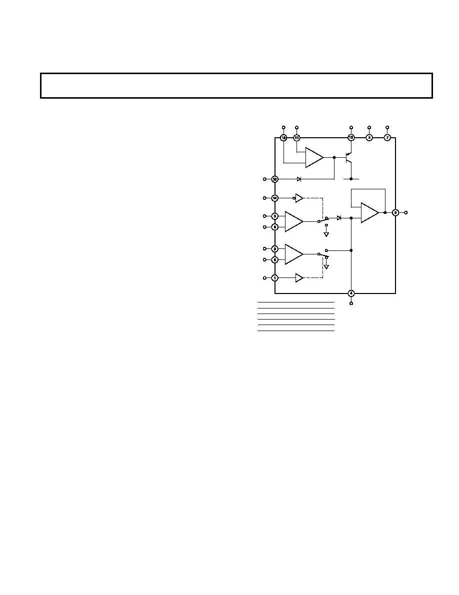
FUNCTIONAL BLOCK DIAGRAM
–
+
PKD01
OUTPUT
BUFFER
OUTPUT
LOGIC
GND
CH
DET
–IN
+IN
–IN
+IN
RST
–IN
+IN
OUTPUT
V+
V–
–
+
–
+
–
+
CMP
A
B
C
V–
D1
GATED
"gm"
AMP
GATED
"gm"
AMP
RST
0
1
DET
0
1
0
OPERATIONAL MODE
PEAK DETECT
PEAK HOLD
RESET
INDETERMINATE
SWITCHES SHOWN FOR:
RST = “0,”
DET = “0”
FEATURES
Monolithic Design for Reliability and Low Cost
High Slew Rate: 0.5 V/ s
Low Droop Rate
TA = 25 C: 0.1 mV/ms
TA = 125 C: 10 mV/ms
Low Zero-Scale Error: 4 mV
Digitally Selected Hold and Reset Modes
Reset to Positive or Negative Voltage Levels
Logic Signals TTL and CMOS Compatible
Uncommitted Comparator On-Chip
Available in Die Form
GENERAL DESCRIPTION
The PKD01 tracks an analog input signal until a maximum
amplitude is reached. The maximum value is then retained as a
peak voltage on a hold capacitor. Being a monolithic circuit, the
PKD01 offers significant performance and package density
advantages over hybrid modules and discrete designs without
sacrificing system versatility. The matching characteristics
attained in a monolithic circuit provide inherent advantages
when charge injection and droop rate error reduction are
primary goals.
Innovative design techniques maximize the advantages of mono-
lithic technology. Transconductance (gm) amplifiers were chosen
over conventional voltage amplifier circuit building blocks. The
gm amplifiers simplify internal frequency compensation, minimize
acquisition time and maximize circuit accuracy. Their outputs
are easily switched by low glitch current steering circuits. The
steered outputs are clamped to reduce charge injection errors
upon entering the hold mode or exiting the reset mode. The inher-
ently low zero-scale error is further reduced by active Zener-Zap
trimming to optimize overall accuracy.
The output buffer amplifier features an FET input stage to
reduce droop rate error during lengthy peak hold periods. A bias
current cancellation circuit minimizes droop error at high ambi-
ent temperatures.
Through the
DET control pin, new peaks may either be detected
or ignored. Detected peaks are presented as positive output
levels. Positive or negative peaks may be detected without
additional active circuits, since Amplifier A can operate as an
inverting or noninverting gain stage.
An uncommitted comparator provides many application options.
Status indication and logic shaping/shifting are typical examples.
相關(guān)PDF資料 |
PDF描述 |
|---|---|
| PKD01AY/883 | SPECIALTY ANALOG CIRCUIT, CDIP14 |
| PKD4118SIOD | 1-OUTPUT 16.8 W DC-DC REG PWR SUPPLY MODULE |
| PKD4210SIN | 1-OUTPUT 26 W DC-DC REG PWR SUPPLY MODULE |
| PKD4319SI | 1-OUTPUT 30 W DC-DC REG PWR SUPPLY MODULE |
| PKD4218SIOA | 1-OUTPUT 21 W DC-DC REG PWR SUPPLY MODULE |
相關(guān)代理商/技術(shù)參數(shù) |
參數(shù)描述 |
|---|---|
| PKD01BY | 制造商:Analog Devices 功能描述: |
| PKD01BY/883 | 制造商:未知廠家 制造商全稱:未知廠家 功能描述:Peak Detector |
| PKD01EP | 制造商:Analog Devices 功能描述:Sample and Hold 2-CH 70us 14-Pin PDIP 制造商:Analog Devices 功能描述:SEMICONDUCTORS |
| PKD01EPZ | 制造商:Analog Devices 功能描述:Sample and Hold 2-CH 70us 14-Pin PDIP 制造商:Analog Devices 功能描述:Sample & Hold Amplifier |
| PKD01EY | 制造商:Analog Devices 功能描述: |
發(fā)布緊急采購,3分鐘左右您將得到回復(fù)。