- 您現在的位置:買賣IC網 > PDF目錄376257 > PSD302V-70J (意法半導體) Low Cost Field Programmable Microcontroller Peripherals PDF資料下載
參數資料
| 型號: | PSD302V-70J |
| 廠商: | 意法半導體 |
| 英文描述: | Low Cost Field Programmable Microcontroller Peripherals |
| 中文描述: | 低成本現場可編程微控制器外圍設備 |
| 文件頁數: | 34/85頁 |
| 文件大小: | 691K |
| 代理商: | PSD302V-70J |
第1頁第2頁第3頁第4頁第5頁第6頁第7頁第8頁第9頁第10頁第11頁第12頁第13頁第14頁第15頁第16頁第17頁第18頁第19頁第20頁第21頁第22頁第23頁第24頁第25頁第26頁第27頁第28頁第29頁第30頁第31頁第32頁第33頁當前第34頁第35頁第36頁第37頁第38頁第39頁第40頁第41頁第42頁第43頁第44頁第45頁第46頁第47頁第48頁第49頁第50頁第51頁第52頁第53頁第54頁第55頁第56頁第57頁第58頁第59頁第60頁第61頁第62頁第63頁第64頁第65頁第66頁第67頁第68頁第69頁第70頁第71頁第72頁第73頁第74頁第75頁第76頁第77頁第78頁第79頁第80頁第81頁第82頁第83頁第84頁第85頁
PSD3XX Famly
31
16.
Power
Management
(cont.)
16.3 Turbo Bit (ZPSD only)
The turbo bit is controlled by the MCU at run-time and is accessed through bit zero of the
Power Management Register (PMR). The PMR is located in CSIOPORT space at offset 10h.
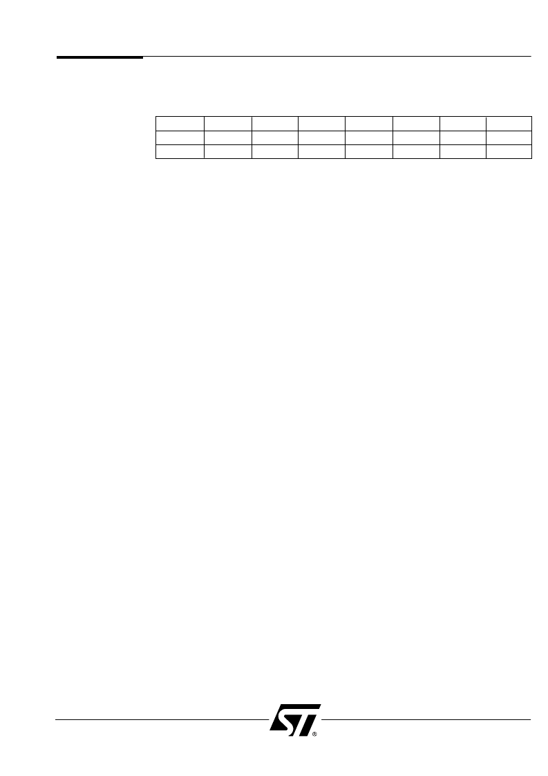
Power Management Register (PMR)
Bit 7
*
1=OFF
Bit 6
*
1=OFF
Bit 5
*
1=OFF
Bit 4
*
1=OFF
Bit 3
*
1=OFF
Bit 2
*
1=OFF
Bit 1
*
1=OFF
Bit 0
Turbo bit
1=OFF
*
Future Configuration bits are reserved and should be set to one when writing to this register.
The default value at reset of all bits in the PMR is logic 0, which means the Turbo feature is
enabled. The PAD logic (PAD A and PAD B) of the PSD will operate at full speed and full
power. When the Turbo Bit is set to logic 1, the Turbo feature is disabled. When disabled,
the PAD logic will draw only standby current (micro-amps) while no PAD inputs change.
Whenever there is a transition on any PAD input (including MCU address and control
signals), the PAD logic will power up and will generate new outputs, latch those outputs,
then go back to Standby Mode. Keep in mind that the signal propagation delay through the
PAD logic increases by 10 nsec for non-V devices, and 20 nsec for V devices while in
non-turbo mode. Use of the Turbo Bit does not affect the operation or power consumption
of memory.
Tremendous power savings are possible by setting the Turbo Bit and going into non-turbo
mode. This essentially reduces the DC power consumption of the PAD logic to zero. It also
reduces the AC power consumption of PAD logic when the composite frequency of all PAD
inputs change at a rate less than 40 MHz for non-V devices, and less than 20 MHz for V
devices. Use Figures 14 and 15 to calculate AC and DC current usage in the PAD with the
Turbo Bit on and off. You will need to know the number of product terms that are used in
your design and you will have to calculate the composite frequency of all signals entering
the PAD logic.
16.4 Number of Product Terms in the PADLogic
The number of product terms used in your design relates directly to how much current the
PADs will draw. Therefore, minimizing this number will be in your best interest if power is a
concern for you. Basically, the amount of product terms your design will use is based on the
following (see Figure 4):
Each of the EPROM block selects, ES0-ES7 uses one product term (for a total of 8).
The CSIOPORT select uses one product term.
If your part has SRAM (non-R versions), the SRAM select RS0 uses one product term.
The Track Mode control signals (CSADIN, CSADOUT1, and CSADOUT2) each use
one product term if you use these signals.
Port B, pins PB0-PB3 are allocated four product terms each if used as outputs.
Port B, pins PB4-PB7 are allocated two product terms each if used as outputs.
Port C, pins PC0-PC2 are allocated one product term each if used as outputs.
Given the above product term allocation, keep the following points in mind when calculating
the total number of product terms your design will require:
1) The EPROM block selects, CSIOPORT select, and SRAM select will use a product term
whether you use these blocks or not. This means you start out with 10 product terms,
and go up from there.
2) For Port B, if you use a pin as an output and your logic equation requires only one
product term, you still have to include all the available product terms for that pin for
power consumption, even though only one product term is specified. For example, if the
output equation for pin PB0 uses just one product term, you will have to count PB0 as
contributing four product terms to the overall count. With this in mind, you should use
Port C for the outputs that only require one product term and PB4-7 for outputs that
require two product terms. Use pins PB0-3 if you need outputs requiring more than two
product terms or you have run out of outputs.
3) The following PSD functions do not consume product terms: MCU I/O mode, Latched
Address Output, and PAD inputs (logic or address).
相關PDF資料 |
PDF描述 |
|---|---|
| PSD302V-70JI | Low Cost Field Programmable Microcontroller Peripherals |
| PSD303R-70JM | Circular Connector; Body Material:Aluminum; Series:PT01; No. of Contacts:41; Connector Shell Size:20; Connecting Termination:Solder; Circular Shell Style:Cable Receptacle; Circular Contact Gender:Pin; Insert Arrangement:20-41 |
| PSD303V-15J | Circular Connector; MIL SPEC:MIL-C-26482, Series I, Solder; Body Material:Aluminum; Series:PT01; No. of Contacts:15; Connector Shell Size:14; Connecting Termination:Solder; Circular Shell Style:Cable Receptacle; Body Style:Straight |
| PSD303V-15JI | Low Cost Field Programmable Microcontroller Peripherals |
| PSD303V-15JM | Low Cost Field Programmable Microcontroller Peripherals |
相關代理商/技術參數 |
參數描述 |
|---|---|
| PSD302V-70JI | 制造商:STMICROELECTRONICS 制造商全稱:STMicroelectronics 功能描述:Low Cost Field Programmable Microcontroller Peripherals |
| PSD302V-70JM | 制造商:STMICROELECTRONICS 制造商全稱:STMicroelectronics 功能描述:Low Cost Field Programmable Microcontroller Peripherals |
| PSD302V-90J | 制造商:STMICROELECTRONICS 制造商全稱:STMicroelectronics 功能描述:Low Cost Field Programmable Microcontroller Peripherals |
| PSD302V-90JI | 制造商:STMICROELECTRONICS 制造商全稱:STMicroelectronics 功能描述:Low Cost Field Programmable Microcontroller Peripherals |
| PSD302V-90JM | 制造商:STMICROELECTRONICS 制造商全稱:STMicroelectronics 功能描述:Low Cost Field Programmable Microcontroller Peripherals |
發布緊急采購,3分鐘左右您將得到回復。