- 您現在的位置:買賣IC網 > PDF目錄376293 > PSD834F5V-15 (意法半導體) Flash In-System Programmable (ISP) Peripherals for 8-bit MCUs, 5V PDF資料下載
參數資料
| 型號: | PSD834F5V-15 |
| 廠商: | 意法半導體 |
| 英文描述: | Flash In-System Programmable (ISP) Peripherals for 8-bit MCUs, 5V |
| 中文描述: | Flash在系統可編程(ISP)的周邊8位MCU,5V的 |
| 文件頁數: | 11/110頁 |
| 文件大小: | 1737K |
| 代理商: | PSD834F5V-15 |
第1頁第2頁第3頁第4頁第5頁第6頁第7頁第8頁第9頁第10頁當前第11頁第12頁第13頁第14頁第15頁第16頁第17頁第18頁第19頁第20頁第21頁第22頁第23頁第24頁第25頁第26頁第27頁第28頁第29頁第30頁第31頁第32頁第33頁第34頁第35頁第36頁第37頁第38頁第39頁第40頁第41頁第42頁第43頁第44頁第45頁第46頁第47頁第48頁第49頁第50頁第51頁第52頁第53頁第54頁第55頁第56頁第57頁第58頁第59頁第60頁第61頁第62頁第63頁第64頁第65頁第66頁第67頁第68頁第69頁第70頁第71頁第72頁第73頁第74頁第75頁第76頁第77頁第78頁第79頁第80頁第81頁第82頁第83頁第84頁第85頁第86頁第87頁第88頁第89頁第90頁第91頁第92頁第93頁第94頁第95頁第96頁第97頁第98頁第99頁第100頁第101頁第102頁第103頁第104頁第105頁第106頁第107頁第108頁第109頁第110頁
11/110
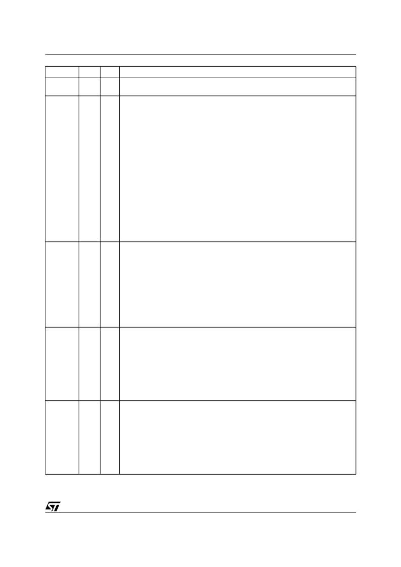
PSD813F2, PSD833F2, PSD834F2, PSD853F2, PSD854F2
Reset
48
I
Resets I/O Ports, PLD macrocells and some of the Configuration Registers. Must be Low
at Power-up.
PA0
PA1
PA2
PA3
PA4
PA5
PA6
PA7
29
28
27
25
24
23
22
21
I/O
These pins make up Port A. These port pins are configurable and can have the following
functions:
MCU I/O – write to or read from a standard output or input port.
CPLD macrocell (McellAB0-7) outputs.
Inputs to the PLDs.
Latched address outputs (see Table
6
).
Address inputs. For example, PA0-3 could be used for A0-A3 when using an 80C51XA in
burst mode.
As the data bus inputs D0-D7 for non-multiplexed address/data bus MCUs.
D0/A16-D3/A19 in M37702M2 mode.
Peripheral I/O mode.
Note:
PA0-PA3 can only output CMOS signals with an option for high slew rate. However,
PA4-PA7 can be configured as CMOS or Open Drain Outputs.
PB0
PB1
PB2
PB3
PB4
PB5
PB6
PB7
7
6
5
4
3
2
52
51
I/O
These pins make up Port B. These port pins are configurable and can have the following
functions:
MCU I/O – write to or read from a standard output or input port.
CPLD macrocell (McellAB0-7 or McellBC0-7) outputs.
Inputs to the PLDs.
Latched address outputs (see Table
6
).
Note:
PB0-PB3 can only output CMOS signals with an option for high slew rate.
However, PB4-PB7 can be configured as CMOS or Open Drain Outputs.
PC0
20
I/O
PC0 pin of Port C. This port pin can be configured to have the following functions:
MCU I/O – write to or read from a standard output or input port.
CPLD macrocell (McellBC0) output.
Input to the PLDs.
TMS Input
2
for the JTAG Serial Interface.
This pin can be configured as a CMOS or Open Drain output.
PC1
19
I/O
PC1 pin of Port C. This port pin can be configured to have the following functions:
MCU I/O – write to or read from a standard output or input port.
CPLD macrocell (McellBC1) output.
Input to the PLDs.
TCK Input
2
for the JTAG Serial Interface.
This pin can be configured as a CMOS or Open Drain output.
Pin Name
Pin
Type
Description
相關PDF資料 |
PDF描述 |
|---|---|
| PSD853F2-12 | Flash In-System Programmable (ISP) Peripherals for 8-bit MCUs, 5V |
| PSD853F2-15 | Flash In-System Programmable (ISP) Peripherals for 8-bit MCUs, 5V |
| PSD853F2-20 | Flash In-System Programmable (ISP) Peripherals for 8-bit MCUs, 5V |
| PSD853F2-70 | Flash In-System Programmable (ISP) Peripherals for 8-bit MCUs, 5V |
| PSD853F2-90 | Flash In-System Programmable (ISP) Peripherals for 8-bit MCUs, 5V |
相關代理商/技術參數 |
參數描述 |
|---|---|
| PSD835G2-70U | 功能描述:靜態隨機存取存儲器 5.0V 4M 70ns RoHS:否 制造商:Cypress Semiconductor 存儲容量:16 Mbit 組織:1 M x 16 訪問時間:55 ns 電源電壓-最大:3.6 V 電源電壓-最小:2.2 V 最大工作電流:22 uA 最大工作溫度:+ 85 C 最小工作溫度:- 40 C 安裝風格:SMD/SMT 封裝 / 箱體:TSOP-48 封裝:Tray |
| PSD835G2-90U | 功能描述:靜態隨機存取存儲器 5.0V 4M 90ns RoHS:否 制造商:Cypress Semiconductor 存儲容量:16 Mbit 組織:1 M x 16 訪問時間:55 ns 電源電壓-最大:3.6 V 電源電壓-最小:2.2 V 最大工作電流:22 uA 最大工作溫度:+ 85 C 最小工作溫度:- 40 C 安裝風格:SMD/SMT 封裝 / 箱體:TSOP-48 封裝:Tray |
| PSD835G2-90UI | 功能描述:靜態隨機存取存儲器 5.0V 4M 90ns RoHS:否 制造商:Cypress Semiconductor 存儲容量:16 Mbit 組織:1 M x 16 訪問時間:55 ns 電源電壓-最大:3.6 V 電源電壓-最小:2.2 V 最大工作電流:22 uA 最大工作溫度:+ 85 C 最小工作溫度:- 40 C 安裝風格:SMD/SMT 封裝 / 箱體:TSOP-48 封裝:Tray |
| PSD835G2V-12UI | 功能描述:靜態隨機存取存儲器 3.0V 4M 120ns RoHS:否 制造商:Cypress Semiconductor 存儲容量:16 Mbit 組織:1 M x 16 訪問時間:55 ns 電源電壓-最大:3.6 V 電源電壓-最小:2.2 V 最大工作電流:22 uA 最大工作溫度:+ 85 C 最小工作溫度:- 40 C 安裝風格:SMD/SMT 封裝 / 箱體:TSOP-48 封裝:Tray |
| PSD835G2V-90U | 功能描述:靜態隨機存取存儲器 3.0V 4M 90ns RoHS:否 制造商:Cypress Semiconductor 存儲容量:16 Mbit 組織:1 M x 16 訪問時間:55 ns 電源電壓-最大:3.6 V 電源電壓-最小:2.2 V 最大工作電流:22 uA 最大工作溫度:+ 85 C 最小工作溫度:- 40 C 安裝風格:SMD/SMT 封裝 / 箱體:TSOP-48 封裝:Tray |
發布緊急采購,3分鐘左右您將得到回復。