- 您現在的位置:買賣IC網 > PDF目錄376281 > PSD8532V12MIT (意法半導體) High Speed CMOS Logic Triple 3-Input NAND Gates 14-PDIP -55 to 125 PDF資料下載
參數資料
| 型號: | PSD8532V12MIT |
| 廠商: | 意法半導體 |
| 英文描述: | High Speed CMOS Logic Triple 3-Input NAND Gates 14-PDIP -55 to 125 |
| 中文描述: | Flash在系統可編程ISP的外設的8位微控制器 |
| 文件頁數: | 67/110頁 |
| 文件大小: | 1737K |
| 代理商: | PSD8532V12MIT |
第1頁第2頁第3頁第4頁第5頁第6頁第7頁第8頁第9頁第10頁第11頁第12頁第13頁第14頁第15頁第16頁第17頁第18頁第19頁第20頁第21頁第22頁第23頁第24頁第25頁第26頁第27頁第28頁第29頁第30頁第31頁第32頁第33頁第34頁第35頁第36頁第37頁第38頁第39頁第40頁第41頁第42頁第43頁第44頁第45頁第46頁第47頁第48頁第49頁第50頁第51頁第52頁第53頁第54頁第55頁第56頁第57頁第58頁第59頁第60頁第61頁第62頁第63頁第64頁第65頁第66頁當前第67頁第68頁第69頁第70頁第71頁第72頁第73頁第74頁第75頁第76頁第77頁第78頁第79頁第80頁第81頁第82頁第83頁第84頁第85頁第86頁第87頁第88頁第89頁第90頁第91頁第92頁第93頁第94頁第95頁第96頁第97頁第98頁第99頁第100頁第101頁第102頁第103頁第104頁第105頁第106頁第107頁第108頁第109頁第110頁
67/110
PSD813F2, PSD833F2, PSD834F2, PSD853F2, PSD854F2
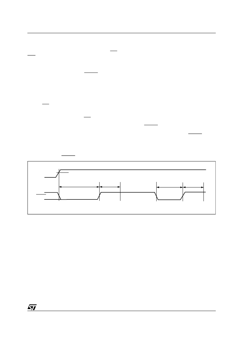
RESET TIMING AND DEVICE STATUS AT RESET
Power-Up Reset
Upon Power-up, the PSD requires a Reset (RE-
SET) pulse of duration t
NLNH-PO
after V
CC
is
steady. During this period, the device loads inter-
nal configurations, clears some of the registers
and sets the Flash memory into Operating mode.
After the rising edge of Reset (RESET), the PSD
remains in the Reset mode for an additional peri-
od, t
OPR
, before the first memory access is al-
lowed.
The Flash memory is reset to the READ Mode
upon Power-up. Sector Select (FS0-FS7 and
CSBOOT0-CSBOOT3) must all be Low, Write
Strobe (WR, CNTL0) High, during Power On Re-
set for maximum security of the data contents and
to remove the possibility of a byte being written on
the first edge of Write Strobe (WR, CNTL0). Any
Flash memory WRITE cycle initiation is prevented
automatically when V
CC
is below V
LKO
.
Warm Reset
Once the device is up and running, the device can
be reset with a pulse of a much shorter duration,
t
NLNH
.
The same t
OPR
period is needed before the device
is operational after warm reset. Figure
34
shows
the timing of the Power-up and warm reset.
I/O Pin, Register and PLD Status at Reset
Table 33., page 68
shows the I/O pin, register and
PLD status during Power On Reset, warm reset
and Power-down mode. PLD outputs are always
valid during warm reset, and they are valid in Pow-
er On Reset once the internal PSD Configuration
bits are loaded. This loading of PSD is completed
typically long before the V
CC
ramps up to operat-
ing level. Once the PLD is active, the state of the
outputs are determined by the PSDabel equa-
tions.
Reset of Flash Memory Erase and Program
Cycles (on the PSD834Fx)
A Reset (RESET) also resets the internal Flash
memory state machine. During a Flash memory
Program or Erase cycle, Reset (RESET) termi-
nates the cycle and returns the Flash memory to
the Read Mode within a period of t
NLNH-A
.
Figure 34. Reset (RESET) Timing
tNLNH-PO
Power-On Reset
tOPR
AI02866b
RESET
tNLNH
tNLNH-A
Warm Reset
tOPR
V
CC
V
CC
(min)
相關PDF資料 |
PDF描述 |
|---|---|
| PSD8532V12MT | High Speed CMOS Logic Triple 3-Input NAND Gates 14-PDIP -55 to 125 |
| PSD8532V15JT | High Speed CMOS Logic Triple 3-Input NAND Gates 14-SOIC -55 to 125 |
| PSD8532V15MT | High Speed CMOS Logic Triple 3-Input NAND Gates 14-SOIC -55 to 125 |
| PSD8532V20JT | High Speed CMOS Logic Triple 3-Input NAND Gates 14-SOIC -55 to 125 |
| PSD833212JIT | Flash In-System Programmable ISP Peripherals For 8-bit MCUs |
相關代理商/技術參數 |
參數描述 |
|---|---|
| PSD853F2-70J | 功能描述:SPLD - 簡單可編程邏輯器件 5.0V 1M 70ns RoHS:否 制造商:Texas Instruments 邏輯系列:TICPAL22V10Z 大電池數量:10 最大工作頻率:66 MHz 延遲時間:25 ns 工作電源電壓:4.75 V to 5.25 V 電源電流:100 uA 最大工作溫度:+ 75 C 最小工作溫度:0 C 安裝風格:Through Hole 封裝 / 箱體:DIP-24 |
| PSD853F2-70M | 功能描述:CPLD - 復雜可編程邏輯器件 5.0V 1M 70ns RoHS:否 制造商:Lattice 系列: 存儲類型:EEPROM 大電池數量:128 最大工作頻率:333 MHz 延遲時間:2.7 ns 可編程輸入/輸出端數量:64 工作電源電壓:3.3 V 最大工作溫度:+ 90 C 最小工作溫度:0 C 封裝 / 箱體:TQFP-100 |
| PSD853F2-90J | 功能描述:CPLD - 復雜可編程邏輯器件 5.0V 1M 90ns RoHS:否 制造商:Lattice 系列: 存儲類型:EEPROM 大電池數量:128 最大工作頻率:333 MHz 延遲時間:2.7 ns 可編程輸入/輸出端數量:64 工作電源電壓:3.3 V 最大工作溫度:+ 90 C 最小工作溫度:0 C 封裝 / 箱體:TQFP-100 |
| PSD853F2-90JI | 功能描述:CPLD - 復雜可編程邏輯器件 5.0V 1M 90ns RoHS:否 制造商:Lattice 系列: 存儲類型:EEPROM 大電池數量:128 最大工作頻率:333 MHz 延遲時間:2.7 ns 可編程輸入/輸出端數量:64 工作電源電壓:3.3 V 最大工作溫度:+ 90 C 最小工作溫度:0 C 封裝 / 箱體:TQFP-100 |
| PSD853F2-90M | 功能描述:CPLD - 復雜可編程邏輯器件 5.0V 1M 90ns RoHS:否 制造商:Lattice 系列: 存儲類型:EEPROM 大電池數量:128 最大工作頻率:333 MHz 延遲時間:2.7 ns 可編程輸入/輸出端數量:64 工作電源電壓:3.3 V 最大工作溫度:+ 90 C 最小工作溫度:0 C 封裝 / 箱體:TQFP-100 |
發布緊急采購,3分鐘左右您將得到回復。