- 您現在的位置:買賣IC網 > PDF目錄376260 > PSD853F5V-70 (意法半導體) Flash In-System Programmable (ISP) Peripherals for 8-bit MCUs, 5V PDF資料下載
參數資料
| 型號: | PSD853F5V-70 |
| 廠商: | 意法半導體 |
| 英文描述: | Flash In-System Programmable (ISP) Peripherals for 8-bit MCUs, 5V |
| 中文描述: | Flash在系統可編程(ISP)的周邊8位MCU,5V的 |
| 文件頁數: | 57/110頁 |
| 文件大?。?/td> | 1737K |
| 代理商: | PSD853F5V-70 |
第1頁第2頁第3頁第4頁第5頁第6頁第7頁第8頁第9頁第10頁第11頁第12頁第13頁第14頁第15頁第16頁第17頁第18頁第19頁第20頁第21頁第22頁第23頁第24頁第25頁第26頁第27頁第28頁第29頁第30頁第31頁第32頁第33頁第34頁第35頁第36頁第37頁第38頁第39頁第40頁第41頁第42頁第43頁第44頁第45頁第46頁第47頁第48頁第49頁第50頁第51頁第52頁第53頁第54頁第55頁第56頁當前第57頁第58頁第59頁第60頁第61頁第62頁第63頁第64頁第65頁第66頁第67頁第68頁第69頁第70頁第71頁第72頁第73頁第74頁第75頁第76頁第77頁第78頁第79頁第80頁第81頁第82頁第83頁第84頁第85頁第86頁第87頁第88頁第89頁第90頁第91頁第92頁第93頁第94頁第95頁第96頁第97頁第98頁第99頁第100頁第101頁第102頁第103頁第104頁第105頁第106頁第107頁第108頁第109頁第110頁
57/110
PSD813F2, PSD833F2, PSD834F2, PSD853F2, PSD854F2
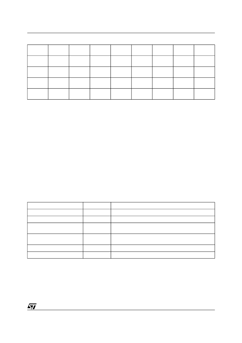
Table 26. Drive Register Pin Assignment
Note: 1. NA = Not Applicable.
Port Data Registers
The Port Data Registers, shown in Table
27
, are
used by the MCU to write data to or read data from
the ports. Table
27
shows the register name, the
ports having each register type, and MCU access
for each register type. The registers are described
below.
Data In
Port pins are connected directly to the Data In buff-
er. In MCU I/O input mode, the pin input is read
through the Data In buffer.
Data Out Register
Stores output data written by the MCU in the MCU
I/O output mode. The contents of the Register are
driven out to the pins if the Direction Register or
the output enable product term is set to ’1.’ The
contents of the register can also be read back by
the MCU.
Output Macrocells (OMC).
The CPLD Output
Macrocells (OMC) occupy a location in the MCU’s
address space. The MCU can read the output of
the Output Macrocells (OMC). If the OMC Mask
Register bits are not set, writing to the macrocell
loads data to the macrocell flip-flops. See the sec-
tion entitled
PLDS, page 33
.
OMC Mask Register
Each OMC Mask Register bit corresponds to an
Output Macrocell (OMC) flip-flop. When the OMC
Mask Register bit is set to a 1, loading data into the
Output Macrocell (OMC) flip-flop is blocked. The
default value is 0 or unblocked.
Table 27. Port Data Registers
Drive
Register
Bit 7
Bit 6
Bit 5
Bit 4
Bit 3
Bit 2
Bit 1
Bit 0
Port A
Open
Drain
Open
Drain
Open
Drain
Open
Drain
Slew
Rate
Slew
Rate
Slew
Rate
Slew
Rate
Port B
Open
Drain
Open
Drain
Open
Drain
Open
Drain
Slew
Rate
Slew
Rate
Slew
Rate
Slew
Rate
Port C
Open
Drain
Open
Drain
Open
Drain
Open
Drain
Open
Drain
Open
Drain
Open
Drain
Open
Drain
Port D
NA
1
NA
1
NA
1
NA
1
NA
1
Slew
Rate
Slew
Rate
Slew
Rate
Register Name
Port
MCU Access
Data In
A,B,C,D
READ – input on pin
Data Out
A,B,C,D
WRITE/READ
Output Macrocell
A,B,C
READ – outputs of macrocells
WRITE – loading macrocells flip-flop
Mask Macrocell
A,B,C
WRITE/READ – prevents loading into a given
macrocell
Input Macrocell
A,B,C
READ – outputs of the Input Macrocells
Enable Out
A,B,C
READ – the output enable control of the port driver
相關PDF資料 |
PDF描述 |
|---|---|
| PSD853F5V-90 | Flash In-System Programmable (ISP) Peripherals for 8-bit MCUs, 5V |
| PSD854F2 | Flash In-System Programmable ISP Peripherals For 8-bit MCUs |
| PSD854F2-12 | Flash In-System Programmable (ISP) Peripherals for 8-bit MCUs, 5V |
| PSD854F2-15 | Flash In-System Programmable (ISP) Peripherals for 8-bit MCUs, 5V |
| PSD854F2-20 | Flash In-System Programmable (ISP) Peripherals for 8-bit MCUs, 5V |
相關代理商/技術參數 |
參數描述 |
|---|---|
| PSD854F2-15J | 制造商:STMicroelectronics 功能描述:4556DIE2HR - Trays |
| PSD854F2-70J | 功能描述:CPLD - 復雜可編程邏輯器件 5.0V 2M 70ns RoHS:否 制造商:Lattice 系列: 存儲類型:EEPROM 大電池數量:128 最大工作頻率:333 MHz 延遲時間:2.7 ns 可編程輸入/輸出端數量:64 工作電源電壓:3.3 V 最大工作溫度:+ 90 C 最小工作溫度:0 C 封裝 / 箱體:TQFP-100 |
| PSD854F2-70M | 功能描述:CPLD - 復雜可編程邏輯器件 5.0V 2M 70ns RoHS:否 制造商:Lattice 系列: 存儲類型:EEPROM 大電池數量:128 最大工作頻率:333 MHz 延遲時間:2.7 ns 可編程輸入/輸出端數量:64 工作電源電壓:3.3 V 最大工作溫度:+ 90 C 最小工作溫度:0 C 封裝 / 箱體:TQFP-100 |
| PSD854F2-90J | 功能描述:CPLD - 復雜可編程邏輯器件 5.0V 2M 90ns RoHS:否 制造商:Lattice 系列: 存儲類型:EEPROM 大電池數量:128 最大工作頻率:333 MHz 延遲時間:2.7 ns 可編程輸入/輸出端數量:64 工作電源電壓:3.3 V 最大工作溫度:+ 90 C 最小工作溫度:0 C 封裝 / 箱體:TQFP-100 |
| PSD854F2-90JI | 功能描述:CPLD - 復雜可編程邏輯器件 5.0V 2M 90ns RoHS:否 制造商:Lattice 系列: 存儲類型:EEPROM 大電池數量:128 最大工作頻率:333 MHz 延遲時間:2.7 ns 可編程輸入/輸出端數量:64 工作電源電壓:3.3 V 最大工作溫度:+ 90 C 最小工作溫度:0 C 封裝 / 箱體:TQFP-100 |
發布緊急采購,3分鐘左右您將得到回復。