- 您現在的位置:買賣IC網 > PDF目錄376296 > PSD9133V70JT (意法半導體) Flash In-System Programmable ISP Peripherals For 8-bit MCUs PDF資料下載
參數資料
| 型號: | PSD9133V70JT |
| 廠商: | 意法半導體 |
| 英文描述: | Flash In-System Programmable ISP Peripherals For 8-bit MCUs |
| 中文描述: | Flash在系統可編程ISP的外設的8位微控制器 |
| 文件頁數: | 30/110頁 |
| 文件大小: | 1737K |
| 代理商: | PSD9133V70JT |
第1頁第2頁第3頁第4頁第5頁第6頁第7頁第8頁第9頁第10頁第11頁第12頁第13頁第14頁第15頁第16頁第17頁第18頁第19頁第20頁第21頁第22頁第23頁第24頁第25頁第26頁第27頁第28頁第29頁當前第30頁第31頁第32頁第33頁第34頁第35頁第36頁第37頁第38頁第39頁第40頁第41頁第42頁第43頁第44頁第45頁第46頁第47頁第48頁第49頁第50頁第51頁第52頁第53頁第54頁第55頁第56頁第57頁第58頁第59頁第60頁第61頁第62頁第63頁第64頁第65頁第66頁第67頁第68頁第69頁第70頁第71頁第72頁第73頁第74頁第75頁第76頁第77頁第78頁第79頁第80頁第81頁第82頁第83頁第84頁第85頁第86頁第87頁第88頁第89頁第90頁第91頁第92頁第93頁第94頁第95頁第96頁第97頁第98頁第99頁第100頁第101頁第102頁第103頁第104頁第105頁第106頁第107頁第108頁第109頁第110頁
PSD813F2, PSD833F2, PSD834F2, PSD853F2, PSD854F2
30/110
SECTOR SELECT AND SRAM SELECT
Sector Select (FS0-FS7, CSBOOT0-CSBOOT3)
and SRAM Select (RS0) are all outputs of the
DPLD. They are setup by writing equations for
them in PSDabel. The following rules apply to the
equations for these signals:
1.
Primary Flash memory and secondary Flash
memory Sector Select signals must
not
be
larger than the physical sector size.
2.
Any primary Flash memory sector must
not
be
mapped in the same memory space as
another Flash memory sector.
3.
A secondary Flash memory sector must
not
be
mapped in the same memory space as
another secondary Flash memory sector.
4.
SRAM, I/O, and Peripheral I/O spaces must
not
overlap.
5.
A secondary Flash memory sector
may
overlap a primary Flash memory sector. In
case of overlap, priority is given to the
secondary Flash memory sector.
6.
SRAM, I/O, and Peripheral I/O spaces
may
overlap any other memory sector. Priority is
given to the SRAM, I/O, or Peripheral I/O.
Example
FS0 is valid when the address is in the range of
8000h to BFFFh, CSBOOT0 is valid from 8000h to
9FFFh, and RS0 is valid from 8000h to 87FFh.
Any address in the range of RS0 always accesses
the SRAM. Any address in the range of CSBOOT0
greater than 87FFh (and less than 9FFFh) auto-
matically addresses secondary Flash memory
segment 0. Any address greater than 9FFFh ac-
cesses the primary Flash memory segment 0. You
can see that half of the primary Flash memory seg-
ment 0 and one-fourth of secondary Flash memory
segment 0 cannot be accessed in this example.
Also note that an equation that defined FS1 to any-
where in the range of 8000h to BFFFh would
not
be valid.
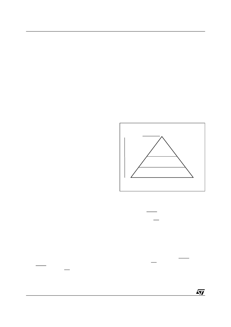
Figure
9
shows the priority levels for all memory
components. Any component on a higher level can
overlap and has priority over any component on a
lower level. Components on the same level must
not
overlap. Level one has the highest priority and
level 3 has the lowest.
Memory Select Configuration for MCUs with
Separate Program and Data Spaces
The 8031 and compatible family of MCUs, which
includes the 80C51, 80C151, 80C251, and
80C51XA, have separate address spaces for Pro-
gram memory (selected using Program Select En-
able (PSEN, CNTL2)) and Data memory (selected
using Read Strobe (RD, CNTL1)). Any of the
memories within the PSD can reside in either
space or both spaces.
This is controlled through manipulation of the VM
register that resides in the CSIOP space.
The VM register is set using PSDsoft Express to
have an initial value. It can subsequently be
changed by the MCU so that memory mapping
can be changed on-the-fly.
For example, you may wish to have SRAM and pri-
mary Flash memory in the Data space at Boot-up,
and secondary Flash memory in the Program
space at Boot-up, and later swap the primary and
secondary Flash memories. This is easily done
with the VM register by using PSDsoft Express
Configuration to configure it for Boot-up and hav-
ing the MCU change it when desired.
Table
13., page 31
describes the VM Register.
Figure 9. Priority Level of Memory and I/O
Components
Configuration Modes for MCUs with Separate
Program and Data Spaces
Separate Space Modes.
Program space is sep-
arated from Data space. For example, Program
Select Enable (PSEN, CNTL2) is used to access
the program code from the primary Flash memory,
while Read Strobe (RD, CNTL1) is used to access
data from the secondary Flash memory, SRAM
and I/O Port blocks. This configuration requires
the VM register to be set to 0Ch (see
Figure
10., page 31
).
Combined Space Modes.
The
Data spaces are combined into one memory
space that allows the primary Flash memory, sec-
ondary Flash memory, and SRAM to be accessed
by either Program Select Enable (PSEN, CNTL2)
or Read Strobe (RD, CNTL1). For example, to
configure the primary Flash memory in Combined
space, Bits b2 and b4 of the VM register are set to
'1' (see
Figure 11., page 31
).
Program
and
Level 1
SRAM, I/O, or
Peripheral I/O
Level 2
Secondary
Non-Volatile Memory
Highest Priority
Lowest Priority
Level 3
Primary Flash Memory
AI02867D
相關PDF資料 |
PDF描述 |
|---|---|
| PSD8333V70JT | Flash In-System Programmable ISP Peripherals For 8-bit MCUs |
| PSD9333V70JT | Flash In-System Programmable ISP Peripherals For 8-bit MCUs |
| PSD8533V70JT | Flash In-System Programmable ISP Peripherals For 8-bit MCUs |
| PSD9533V70JT | Flash In-System Programmable ISP Peripherals For 8-bit MCUs |
| PSD8143V70JT | Flash In-System Programmable ISP Peripherals For 8-bit MCUs |
相關代理商/技術參數 |
參數描述 |
|---|---|
| PSD9133V70MIT | 制造商:STMICROELECTRONICS 制造商全稱:STMicroelectronics 功能描述:Flash In-System Programmable ISP Peripherals For 8-bit MCUs |
| PSD9133V70MT | 制造商:STMICROELECTRONICS 制造商全稱:STMicroelectronics 功能描述:Flash In-System Programmable ISP Peripherals For 8-bit MCUs |
| PSD9133V90JIT | 制造商:STMICROELECTRONICS 制造商全稱:STMicroelectronics 功能描述:Flash In-System Programmable ISP Peripherals For 8-bit MCUs |
| PSD9133V90JT | 制造商:STMICROELECTRONICS 制造商全稱:STMicroelectronics 功能描述:Flash In-System Programmable ISP Peripherals For 8-bit MCUs |
| PSD9133V90MIT | 制造商:STMICROELECTRONICS 制造商全稱:STMicroelectronics 功能描述:Flash In-System Programmable ISP Peripherals For 8-bit MCUs |
發布緊急采購,3分鐘左右您將得到回復。