- 您現在的位置:買賣IC網 > PDF目錄368340 > PT5041N Analog IC PDF資料下載
參數資料
| 型號: | PT5041N |
| 英文描述: | Analog IC |
| 中文描述: | 模擬IC |
| 文件頁數: | 1/3頁 |
| 文件大小: | 105K |
| 代理商: | PT5041N |
For technical support and more information, see inside back cover or visit www.ti.com
Ordering Information
PT 5041
= +12 Volts
PT 5042
= +15 Volts
PT 5044
= +8 Volts
PT 5045
= +9 Volts
PT 5046
= +10 Volts
PT 5047
= +18 Volts
PT 5048
= +12.6 Volts
PT 5049
= +20 Volts
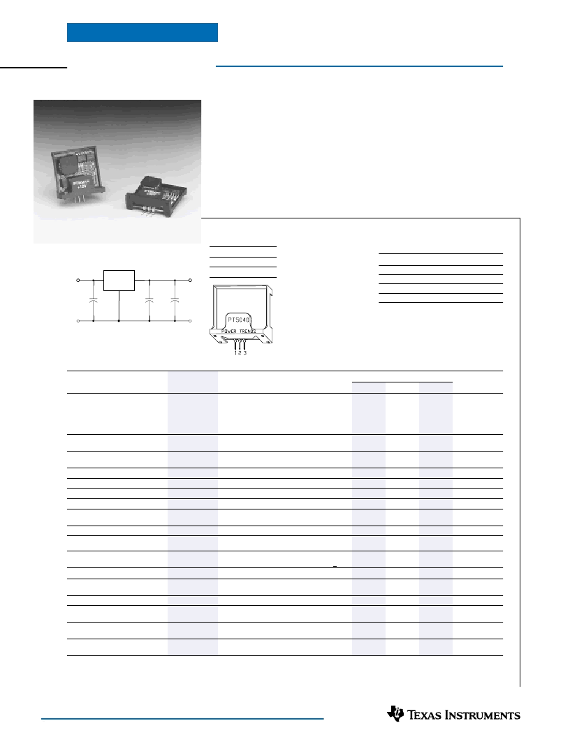
Pin-Out Information
Pin
Function
1
V
in
2
GND
3
V
out
Standard Application
C
1
= Optional ceramic (1-5μF)
C
2
= Optional ceramic (1-5μF)
C
3
= Required Electrolytic (100μF)
NOTE: Boost Topology ISRs are not Short-Circuit Protected.
Features
Wide Input Voltage Range
85% Efficiency
Internal Over-Temperature
Protection
Laser-trimmed Output Voltage
Soft Start
5-Pin Mount Option
(Suffixes L & M)
1-A Positive Step-up
Integrated Switching Regulator
PT5040 Series
SLTS026B
(Revised 12/19/2001)
PT Series Suffix
(PT1234
x
)
Case/Pin
Configuration
Vertical
Horizontal
SMD
Horizontal, 2-pin Tab
SMD, 2-Pin Tab
* Previously known as package styles 100/110.
(Reference the applicable package code drawing
for the dimensions and PC board layout)
Order
Suffix
N
A
C
M
L
Package
C ode *
(EAD)
(EAA)
(EAC)
(EAM)
(EAL)
Description
The PT5040 is a series of 3-pin
boost-voltage Integrated Switching
Regulators (ISRs). These ISRs are
designed for use with +5V bus systems
that require an additional regulated
+8V to +20V with up to 1A of output
current. These ISRs are packaged in
the 3-pin, single in-line pin (SIP)
package configuration.
Specifications
(Unless otherwise stated, T
a
=25°C, V
in
=5V, I
o
=I
o
max, C
3
=100μF)
PT5040 SERIES
Typ
—
—
—
—
—
—
—
—
Characteristics
Output Current
Symbol
I
o
Conditions
Over V
in
range
Min
Max
0.5
0.6
1.0
0.75
1.5
1.2
(V
o
–
1)
14
Units
PT5049
PT5047
PT5041/48
PT5042
PT5044
PT5045/46
0.1
(1)
0.1
(1)
0.1
(1)
0.1
(1)
0.1
(1)
0.1
(1)
4.75
4.75
A
Input Voltage Range
V
in
Over Io range
V
PT5047/5049
Output Voltage Tolerance
V
o
Over V
Range
T
a
= -20°C to SOA derating limit
(3)
Over V
in
range
I
o
min
≤
I
o
≤
I
o
max
I
o
=0.5A
20MHz bandwidth
25% load change
V
o
over/undershoot
—
—
—
—
—
—
—
—
—
±1.5
±0.5
±0.5
85
±2
500
3.0
150
(2)
5.5
(3)
1
650
800
—
40
±3.0
±1.0
±1.0
—
±5
—
5.0
—
—
%V
o
%V
o
%V
o
%
%V
o
μSec
%V
o
%I
o
max
A
mSec
Line Regulation
Load Regulation
Efficiency
V
o
Ripple (pk-pk)
Transient Response
Reg
line
Reg
load
η
V
r
t
tr
V
os
I
lim
I
ir
t
ir
s
Current Limit
Inrush Current
On start up
Switching Frequency
Over V
in
and I
o
ranges
V
o
<15V
V
o
>15V
500
650
-20
—
800
950
+85
(4)
—
kHz
Operating Temperature Range
Thermal Resistance
T
a
θ
ja
—
Free Air Convection
(40-60LFM)
°C
°C/W
Storage Temperature
Mechanical Shock
T
s
-40
—
+125
°C
Per Mil-STD-883D, Method 2002.3
1 msec, Half Sine, mounted to a fixture
Suffixes N, A, & C
Suffixes L & M
Suffixes N, A, & C
Suffixes L & M
—
500
—
—
—
—
—
5
20
(5)
4.5
6.5
G’s
—
—
—
—
Mechanical Vibration
Per Mil-STD-883D, 20-2000 Hz
Weight
G’s
grams
Notes:
(1) The ISR will operate at no load with reduced specifications.
(2) Boost topology ISRs are not short circuit protected.
(3) The inrush current stated is above the normal input current for the associated output load.
(4) See Safe Operating Area curves or consult the factory for the appropriate derating
(5) The tab pins on the 5-pin mount package types (suffixes L & M) must be soldered. For more information see the applicable package outline drawing.
PT5040
3
2
1
C
100μF
+
C
2
+V
out
COM
COM
+V
in
C
1
相關PDF資料 |
PDF描述 |
|---|---|
| PT5042A | Analog IC |
| PT5042C | 30V Single N-Channel HEXFET Power MOSFET in a SO-8 package; Similar to IRF9410 with Lead Free Packaging |
| PT5042L | Analog IC |
| PT5042M | 55V Single N-Channel HEXFET Power MOSFET in a TO-220 FullPak (Iso) package; A IRFI1010N with Standard Packaging |
| PT5042N | 55V Single N-Channel HEXFET Power MOSFET in a TO-220 FullPak (Iso) package; Similar to IRFI1010N with Lead Free Packaging |
相關代理商/技術參數 |
參數描述 |
|---|---|
| PT5041N | 制造商:POWER TRENDS 功能描述:IC ISR VERTICAL +5V 5041 |
| PT5041S | 功能描述:開關變換器、穩壓器與控制器 12Vout 1A 5V-Input Step-Up ISR RoHS:否 制造商:Texas Instruments 輸出電壓:1.2 V to 10 V 輸出電流:300 mA 輸出功率: 輸入電壓:3 V to 17 V 開關頻率:1 MHz 工作溫度范圍: 安裝風格:SMD/SMT 封裝 / 箱體:WSON-8 封裝:Reel |
| PT5042 | 制造商:TI 制造商全稱:Texas Instruments 功能描述:1 AMP STEP-UP INTEGRATED SWITCHING REGULATOR |
| PT5042A | 功能描述:DC/DC轉換器 15Vout 0.75A 5V-Input Step-Up ISR RoHS:否 制造商:Murata 產品: 輸出功率: 輸入電壓范圍:3.6 V to 5.5 V 輸入電壓(標稱): 輸出端數量:1 輸出電壓(通道 1):3.3 V 輸出電流(通道 1):600 mA 輸出電壓(通道 2): 輸出電流(通道 2): 安裝風格:SMD/SMT 封裝 / 箱體尺寸: |
| PT5042C | 功能描述:開關變換器、穩壓器與控制器 15Vout 0.75A 5V-Input Step-Up ISR RoHS:否 制造商:Texas Instruments 輸出電壓:1.2 V to 10 V 輸出電流:300 mA 輸出功率: 輸入電壓:3 V to 17 V 開關頻率:1 MHz 工作溫度范圍: 安裝風格:SMD/SMT 封裝 / 箱體:WSON-8 封裝:Reel |
發布緊急采購,3分鐘左右您將得到回復。