- 您現在的位置:買賣IC網 > PDF目錄361236 > Q67100-H3527 (SIEMENS AG) 4 Kbit 512 x 8 bit Serial CMOS EEPROMs, I2C Synchronous 2-Wire Bus, Page Protection Mode PDF資料下載
參數資料
| 型號: | Q67100-H3527 |
| 廠商: | SIEMENS AG |
| 英文描述: | 4 Kbit 512 x 8 bit Serial CMOS EEPROMs, I2C Synchronous 2-Wire Bus, Page Protection Mode |
| 中文描述: | 4千位512 × 8位串行CMOS EEPROM的,I2C同步2線巴士,頁面保護模式 |
| 文件頁數: | 7/53頁 |
| 文件大小: | 418K |
| 代理商: | Q67100-H3527 |
第1頁第2頁第3頁第4頁第5頁第6頁當前第7頁第8頁第9頁第10頁第11頁第12頁第13頁第14頁第15頁第16頁第17頁第18頁第19頁第20頁第21頁第22頁第23頁第24頁第25頁第26頁第27頁第28頁第29頁第30頁第31頁第32頁第33頁第34頁第35頁第36頁第37頁第38頁第39頁第40頁第41頁第42頁第43頁第44頁第45頁第46頁第47頁第48頁第49頁第50頁第51頁第52頁第53頁
HYB 39S64400/800/160BT(L)
64-MBit Synchronous DRAM
Data Book
7
12.99
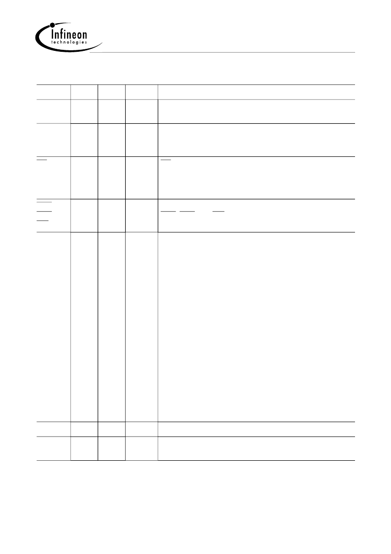
Signal Pin Description
Pin
Type
Signal Polarity Function
CLK
Input
Pulse
Positive
Edge
The System Clock Input. All of the SDRAM inputs are
sampled on the rising edge of the clock.
CKE
Input
Level
Active
High
Activates the CLK signal when high and deactivates the
CLK signal when low, thereby initiates either the Power
Down mode, Suspend mode, or the Self Refresh mode.
CS
Input
Pulse
Active
Low
CS enables the command decoder when low and disables
the command decoder when high. When the command
decoder is disabled, new commands are ignored but
previous operations continue.
RAS
CAS
WE
Input
Pulse
Active
Low
When sampled at the positive rising edge of the clock,
CAS, RAS, and WE define the command to be executed by
the SDRAM.
A0 - A11
Input
Level
–
During a Bank Activate command cycle, A0 - A11 define
the row address (RA0 - RA11) when sampled at the rising
clock edge.
During a Read or Write command cycle, A0-An define the
column address (CA0 - CAn) when sampled at the rising
clock edge.CAn depends from the SDRAM organization:
16M
×
4 SDRAM CAn = CA9
8M
×
8 SDRAM
CAn = CA8
4M
×
16 SDRAM CAn = CA7
(Page Length = 1024 bits)
(Page Length = 512 bits)
(Page Length = 256 bits)
In addition to the column address, A10 (= AP) is used to
invoke autoprecharge operation at the end of the burst read
or write cycle. If A10 is high, autoprecharge is selected and
BA0, BA1 defines the bank to be precharged. If A10 is low,
autoprecharge is disabled.
During a Precharge command cycle, A10 (= AP) is used in
conjunction with BA0 and BA1 to control which bank(s) to
precharge. If A10 is high, all four banks will be precharged
regardless of the state of BA0 and BA1. If A10 is low, then
BA0 and BA1 are used to define which bank to precharge.
BA0, BA1 Input
Level
–
Bank Select Inputs. Selects which bank is to be active.
DQx
Input
Output
Level
–
Data Input/Output pins operate in the same manner as on
conventional DRAMs.
相關PDF資料 |
PDF描述 |
|---|---|
| Q67100-H3528 | 4 Kbit 512 x 8 bit Serial CMOS EEPROMs, I2C Synchronous 2-Wire Bus |
| Q67100-H3529 | 4 Kbit 512 x 8 bit Serial CMOS EEPROMs, I2C Synchronous 2-Wire Bus |
| Q67100-H3530 | 4 Kbit 512 x 8 bit Serial CMOS EEPROMs, I2C Synchronous 2-Wire Bus, Page Protection Mode |
| Q67100-H3531 | 4 Kbit 512 x 8 bit Serial CMOS EEPROMs, I2C Synchronous 2-Wire Bus, Page Protection Mode |
| Q67100-H3532 | 4 Kbit 512 x 8 bit Serial CMOS EEPROMs, I2C Synchronous 2-Wire Bus, Page Protection Mode |
相關代理商/技術參數 |
參數描述 |
|---|---|
| Q67100-H3528 | 制造商:INFINEON 制造商全稱:Infineon Technologies AG 功能描述:4 Kbit 512 x 8 bit Serial CMOS EEPROMs, I2C Synchronous 2-Wire Bus |
| Q67100-H3529 | 制造商:INFINEON 制造商全稱:Infineon Technologies AG 功能描述:4 Kbit 512 x 8 bit Serial CMOS EEPROMs, I2C Synchronous 2-Wire Bus |
| Q67100-H3530 | 制造商:INFINEON 制造商全稱:Infineon Technologies AG 功能描述:4 Kbit 512 x 8 bit Serial CMOS EEPROMs, I2C Synchronous 2-Wire Bus, Page Protection Mode |
| Q67100-H3531 | 制造商:INFINEON 制造商全稱:Infineon Technologies AG 功能描述:4 Kbit 512 x 8 bit Serial CMOS EEPROMs, I2C Synchronous 2-Wire Bus, Page Protection Mode |
| Q67100-H3532 | 制造商:INFINEON 制造商全稱:Infineon Technologies AG 功能描述:4 Kbit 512 x 8 bit Serial CMOS EEPROMs, I2C Synchronous 2-Wire Bus, Page Protection Mode |
發布緊急采購,3分鐘左右您將得到回復。