- 您現在的位置:買賣IC網 > PDF目錄278701 > QL3025-2PB256I Field Programmable Gate Array (FPGA) PDF資料下載
參數資料
| 型號: | QL3025-2PB256I |
| 英文描述: | Field Programmable Gate Array (FPGA) |
| 中文描述: | 現場可編程門陣列(FPGA) |
| 文件頁數: | 1/10頁 |
| 文件大小: | 180K |
| 代理商: | QL3025-2PB256I |
7-27
25,000 Usable PLD Gate pASIC 3 FPGA Combining High Performance and High Density
QL3025 - pASIC 3 FPGATM
QL3025 Rev C
QL3025 - pASIC 3 FPGA
Device Highlights
High Performance & High Density
s
25,000 Usable PLD Gates with 204 I/Os
s
16-bit counter speeds over 300 MHz, data path speeds over
400 MHz
s
0.35um four-layer metal non-volatile CMOS process for
smallest die sizes
Easy to Use / Fast Development Cycles
s
100% routable with 100% utilization and complete
pin-out stability
s
Variable-grain logic cells provide high performance and
100% utilization
s
Comprehensive design tools include high quality
Verilog/VHDL synthesis
Advanced I/O Capabilites
s
Interfaces with both 3.3 volt and 5.0 volt devices
s
PCI compliant with 3.3V and 5.0V buses for -1/-2/-3/-4
speed grades
s
Full JTAG boundary scan
s
Registered I/O cells with individually controlled clocks and
output enables
Total of 204 I/O Pins
s
196 bidirectional input/output pins, PCI-compliant for 5.0 volt
and 3.3 volt buses for -1/-2/-3/-4 speed grades
s
4 high-drive input-only pins
s
4 high-drive input/distributed network pins
Four Low-Skew Distributed Networks
s
Two array clock/control networks available to the logic cell flip-
flop clock, set and reset inputs - each driven by an input-only pin
s
Six global clock/control networks available to the logic cell F1,
clock set and reset inputs and the input and I/O register clock,
reset and enable inputs as well as the output enable control - each
driven by an input-only or I/O pin, or any logic cell output or I/O
cell feedback
High Performance
s
Input + logic cell + output total delays under 6 ns
s
Data path speeds over 400 MHz
s
Counter speeds over 300 MHz
DEVICE HIGHLIGHTS
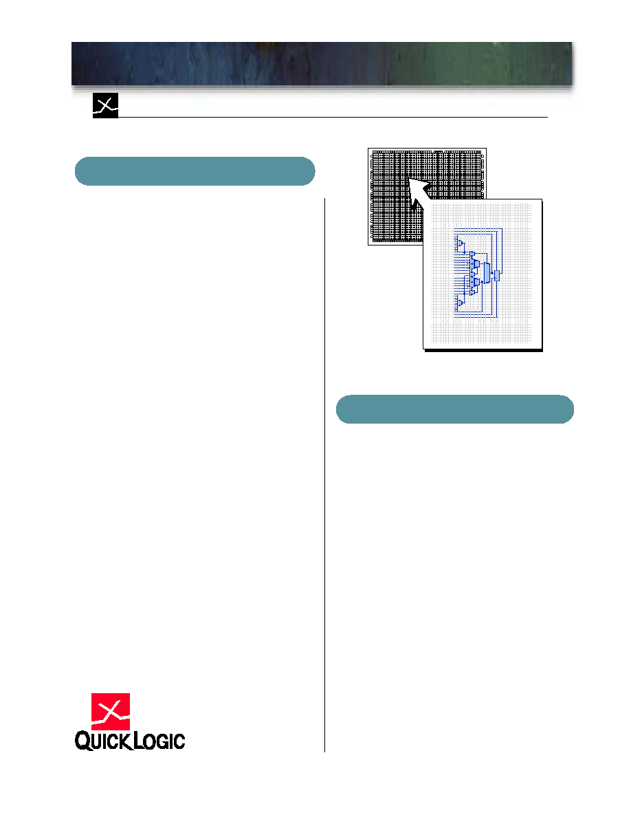
FIGURE 1. 672 Logic Cells
Product Summary
The QL3025 is a 25,000 usable PLD gate member of
the pASIC 3 family of FPGAs. pASIC 3 FPGAs are
fabricated on a 0.35mm four-layer metal process
using QuickLogic’s patented ViaLink technology to
provide a unique combination of high performance,
high density, low cost, and extreme ease-of-use.
The QL3025 contains 672 logic cells. With a
maximum of 204 I/Os, the QL3025 is available in
144-pin TQFP, 208-PQFP, and 256-pin PBGA
packages.
Software support for the complete pASIC 3 family,
including the QL3025, is available through three basic
packages. The turnkey QuickWorks“ package
provides the most complete FPGA software solution
from design entry to logic synthesis, to place and
route, to simulation. The QuickToolsTM for
Workstations package provides a solution for
designers who use Cadence, Exemplar, Mentor,
Synopsys, Synplicity, Viewlogic, Veribest, or other
third-party tools for design entry, synthesis, or
simulation.
PRODUCT SUMMARY
相關PDF資料 |
PDF描述 |
|---|---|
| QL3025-4PF144I | Field Programmable Gate Array (FPGA) |
| QL3025-4PF144M | FPGA |
| QL3025-4PQ208C | Field Programmable Gate Array (FPGA) |
| QL3025-4PQ208I | Field Programmable Gate Array (FPGA) |
| QL3025-4PQ208M | FPGA |
相關代理商/技術參數 |
參數描述 |
|---|---|
| QL30252PB256M | 制造商:未知廠家 制造商全稱:未知廠家 功能描述:25,000 Usable PLD Gate pASIC 3 FPGA Combining High Performance and High Density |
| QL3025-2PB256M | 制造商:未知廠家 制造商全稱:未知廠家 功能描述:Field Programmable Gate Array (FPGA) |
| QL30252PF144C | 制造商:未知廠家 制造商全稱:未知廠家 功能描述:25,000 Usable PLD Gate pASIC 3 FPGA Combining High Performance and High Density |
| QL3025-2PF144C | 制造商:未知廠家 制造商全稱:未知廠家 功能描述:Field Programmable Gate Array (FPGA) |
| QL30252PF144I | 制造商:未知廠家 制造商全稱:未知廠家 功能描述:25,000 Usable PLD Gate pASIC 3 FPGA Combining High Performance and High Density |
發布緊急采購,3分鐘左右您將得到回復。