- 您現在的位置:買賣IC網 > PDF目錄361291 > QL4090-2PQ240C FPGA|1584-CELL|CMOS|QFP|240PIN|PLASTIC PDF資料下載
參數資料
| 型號: | QL4090-2PQ240C |
| 英文描述: | FPGA|1584-CELL|CMOS|QFP|240PIN|PLASTIC |
| 中文描述: | FPGA的| 1584細胞|的CMOS | QFP封裝| 240針腳|塑料 |
| 文件頁數: | 1/12頁 |
| 文件大小: | 290K |
| 代理商: | QL4090-2PQ240C |
6-55
90,000 Usable PLD Gate QuickRAM ESP Combining Performance, Density, and Embedded RAM
QL4090 - QuickRAM
TM
QL4090 Rev G
QL4090 - QuickRAM
Device Highlights
High Performance & High Density
I
90,000 Usable PLD Gates with 316 I/Os
I
300 MHz 16-bit Counters, 400 MHz Datapaths,
160+ MHz FIFOs
I
0.35
μ
m four-layer metal non-volatile CMOS process for
smallest die sizes
High Speed Embedded SRAM
I
22 dual-port RAM modules, organized in user-config-
urable 1,152 bit blocks
I
5ns access times, each port independently accessible
I
Fast and effecient for FIFO, RAM, and ROM functions
Easy to Use / Fast Development Cycles
I
100% routable with 100% utilization and complete
pin-out stability
I
Variable-grain logic cells provide high performance and
100% utilization
I
Comprehensive design tools include high quality
Verilog/VHDL synthesis
Advanced I/O Capabilities
I
Interfaces with both 3.3 volt and 5.0 bolt devices
I
PCI compliant with 3.3V and 5.0V busses for -1/-2/-3/-4
speed grades
I
Full JTAG boundary scan
I
Registered I/O cells with individually controlled clocks and
output enables
D
EVICE
H
IGHLIGHTS
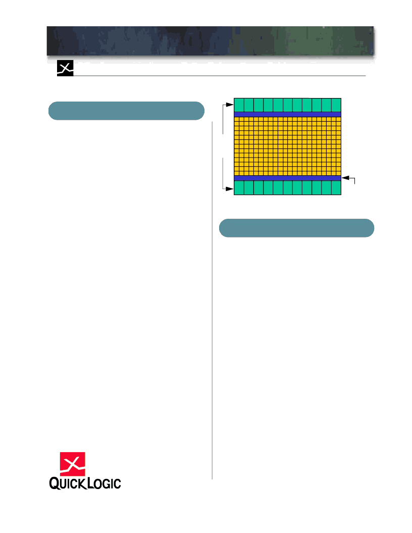
FIGURE 1. QuickRAM Block Diagram
Architecture Overview
The QuickRAM family of ESPs (Embedded Standard
Products) offers FPGA logic in combination with Dual-
Port SRAM modules. The QL4090 is a 90,000
usable PLD gate member of the QuickRAM family of
ESPs. QuickRAM ESPs are fabricated on a 0.35mm
four-layer metal process using QuickLogic’s patented
ViaLink
TM
technology to provide a unique combina-
tion of high performance, high density, low cost, and
extreme ease-of-use.
The QL4090 contains 1,584 logic cells and 22 dual
port RAM modules (see Figure 1). Each RAM module
has 1,152 RAM bits, for a total of 25,344 bits. RAM
Modules are Dual Port (one read port, one write port)
and can be configured into one of four modes: 64
(deep) x18 (wide), 128x9, 256x4, or 512x2 (see Fig-
ure 2). With a maximum of 204 I/Os, the QL4090 is
available in 208-PQFP, 240-pin PQFP and 456-pin
PBGA packages.
Designers can cascade multiple RAM modules to
increase the depth or width allowed in single modules
by connecting corresponding address lines together
and dividing the words between modules (see Figure
3). This approach allows up to 512-deep configura-
tions as large as 16 bits wide in the smallest Quick-
RAM device and 44 bits wide in the largest device.
22
RAM
Blocks
}
1,584
High Speed
Logic Cells
Interface
A
RCHITECTURE
O
VERVIEW
相關PDF資料 |
PDF描述 |
|---|---|
| QL4090-2PQ240I | Field Programmable Gate Array (FPGA) |
| QL4090-2PQ240M | FPGA|1584-CELL|CMOS|QFP|240PIN|PLASTIC |
| QL4090-3PB456C | Field Programmable Gate Array (FPGA) |
| QL4090-3PB456I | FPGA|1584-CELL|CMOS|BGA|456PIN|PLASTIC |
| QL4090-3PQ208C | Field Programmable Gate Array (FPGA) |
相關代理商/技術參數 |
參數描述 |
|---|---|
| QL4090-2PQ240I | 制造商:未知廠家 制造商全稱:未知廠家 功能描述:Field Programmable Gate Array (FPGA) |
| QL4090-2PQ240M | 制造商:未知廠家 制造商全稱:未知廠家 功能描述:FPGA|1584-CELL|CMOS|QFP|240PIN|PLASTIC |
| QL4090-2PQ240M/883 | 制造商:未知廠家 制造商全稱:未知廠家 功能描述:90,000 Usable PLD Gate QuickRAM Combining Performance, Density and Embedded RAM |
| QL4090-3PB456C | 制造商:未知廠家 制造商全稱:未知廠家 功能描述:Field Programmable Gate Array (FPGA) |
| QL4090-3PB456I | 制造商:未知廠家 制造商全稱:未知廠家 功能描述:FPGA|1584-CELL|CMOS|BGA|456PIN|PLASTIC |
發布緊急采購,3分鐘左右您將得到回復。